Plastic ball grid array package for passing JEDEC Level 1 Moisture Sensitivity Test

a technology of pbga package and wafer, which is applied in the direction of electrical equipment, semiconductor devices, semiconductor/solid-state device details, etc., can solve the problems of pbga package failure, very common failure, and level 1 moisture sensitivity test remains extremely challenging

Inactive Publication Date: 2002-07-23
INST OF MICROELECTRONICS A SINGAPORE COMPANY LIMITED BY GUARANTEE
View PDF11 Cites 23 Cited by
  • Summary
  • Abstract
  • Description
  • Claims
  • Application Information

AI Technical Summary

Problems solved by technology

Fractures created in the adhesive material, or delamination at the adhesive-substrate interface are the most common causes of PBGA package failure.
Such a failure is very common in the "popcorn" test which is a moisture sensitivity test.
Some advanced PBGA packages can pass the Level 2 Moisture Sensitivity Test, but the Level 1 Moisture Sensitivity Test remains extremely challenging.
Under certain conditions, the pressure from the expanding moisture and steam can cause internal delamination of the plastic from the chip and / or substrate, internal cracks that do not extend to the outside of the package, band damage, wire necking, bond lifting, thin film cracking, or cratering beneath the bonds.
In the most severe case, the stress can result in external package cracks.
Surface mount devices (SMD) such as PBGA packages are more susceptible to this problem than through-hole parts because they are exposed to higher temperatures during reflow soldering.
The additional steps of either placing the PBGA packages in hermetic bags, or baking them increases the manufacturing cost of a device or a product.
These techniques, which do increase adhesion, all require extra steps and generally add additional production costs.
A drawback with this technique is that the die may not be completely sealed from environmental elements and contaminants.

Method used


Image

  • Plastic ball grid array package for passing JEDEC Level 1 Moisture Sensitivity Test
  • Plastic ball grid array package for passing JEDEC Level 1 Moisture Sensitivity Test
  • Plastic ball grid array package for passing JEDEC Level 1 Moisture Sensitivity Test

Examples


Embodiment Construction

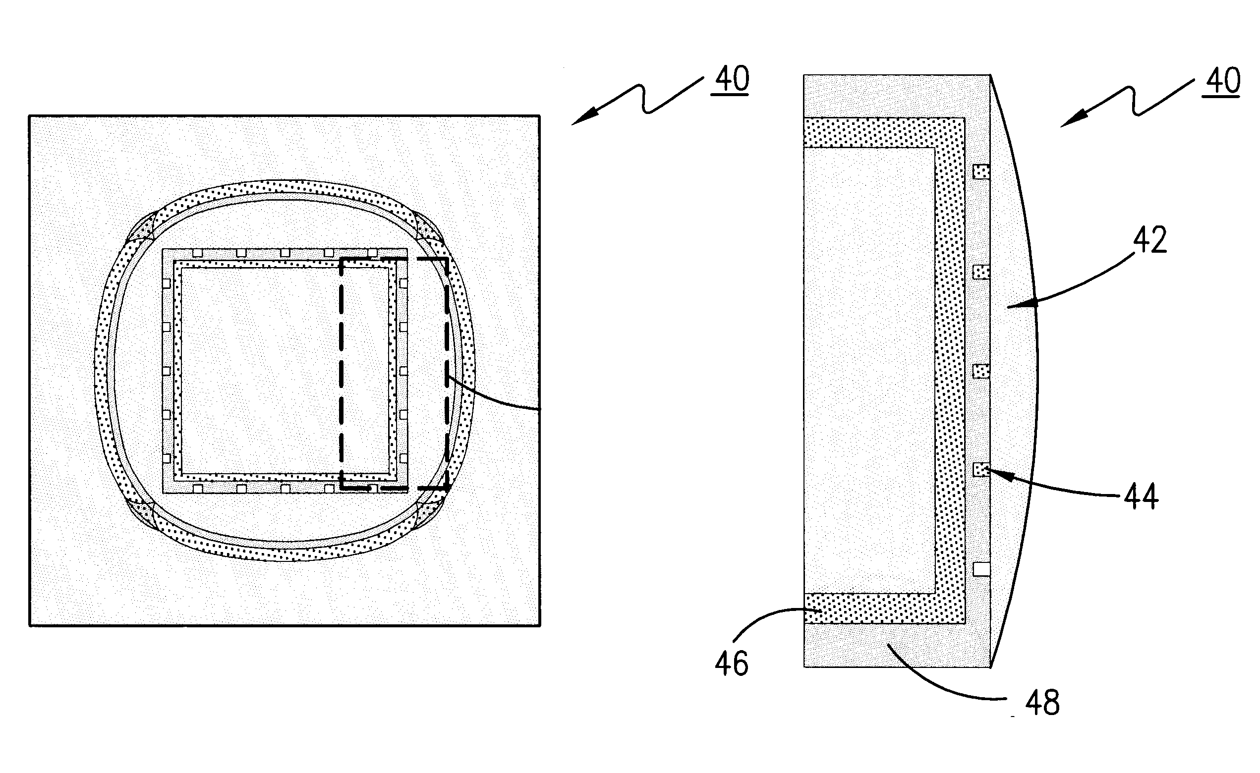
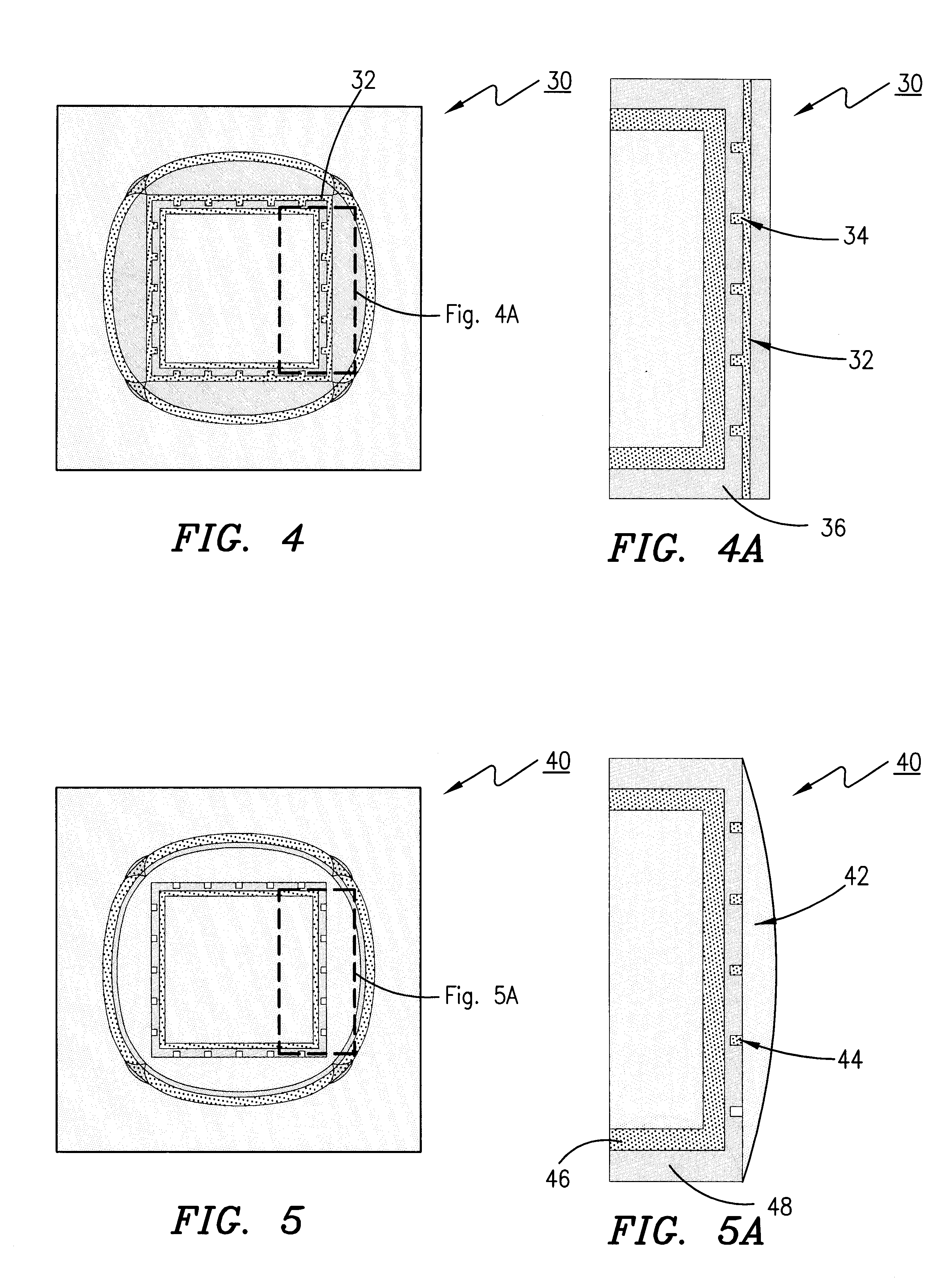
The present invention will now be described more fully hereinafter with reference to the accompanying drawings, in which preferred embodiments of the invention are shown. This invention may, however, be embodied in many different forms and should not be construed as limited to the embodiments set forth herein; rather, these embodiments are provided so that this disclosure will be thorough and complete, and will fully convey the scope of the invention to those skilled in the art.

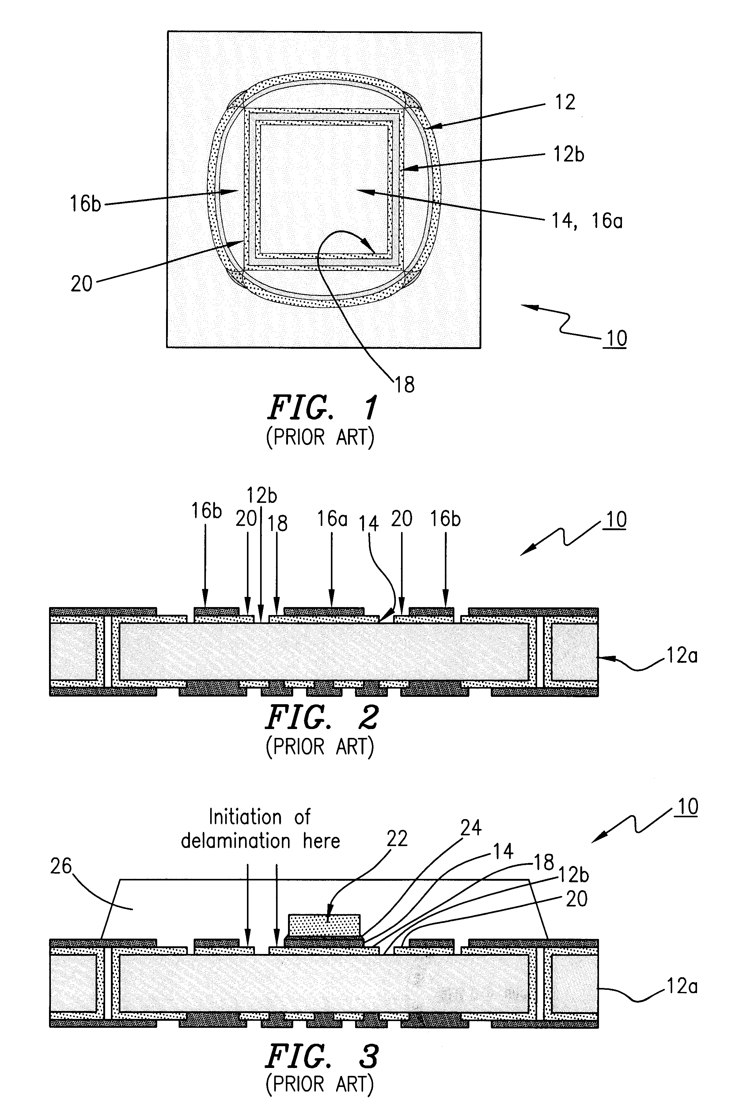
Referring first to FIGS. 1, 2 and 3, wherein conventional or prior art PBGA packages 10 are depicted. A conventional PBGA package has a laminate core / substrate 12. Substantially in the center of the PBGA package 10 is a die pad 14 that is covered with a solder mask 16a. The die pad may be made of copper or another conductive metal. The solder mask 16a covers the die pad 14 so that a continuous square grounding portion (ground ring) 18 is exposed about the die pad 14. The ground ring 18 may be gold plated. The...


PUM


Abstract

A plastic ball grid array package is designed to pass the JEDEC Level 1 Moisture Sensitivity Test (the "popcorn test"). The plastic ball grid array design minimizes contact between a mold compound/encapsulate/glob top and metal surfaces. The present plastic ball grid array design maximizes contact between the mold compound/encapsulate/glob top and either the laminate core or the solder resist in order to take advantage of this strong bond which will help disable delamination. Furthermore, solder resistive material overlaps the interface between metal surfaces and the laminate core.

Description

BACKGROUND OF THE PRESENT INVENTION1. Field of the inventionThe present invention relates generally to integrated circuit carriers and in particular to plastic ball grid array carriers and chip-scale-packaging that is relatively insensitive to delamination when subjected to a moisture sensitivity test commonly referred to as a "popcorn test".2. Description of Related ArtIn a conventional plastic ball grid array (PBGA) package a silicon die is mounted on a die pad of a multilayer organic substrate. The entire die pad area of the substrate is coated with an adhesive which bonds the silicon die to the substrate.Fractures created in the adhesive material, or delamination at the adhesive-substrate interface are the most common causes of PBGA package failure. Such a failure is very common in the "popcorn" test which is a moisture sensitivity test. Conventional PBGA packages can only pass the Institute for Interconnecting and Packaging Electronic Circuits (IPC) and the Joint Election Devic...

Claims


Application Information

Patent Timeline
Patent Type & Authority Patents(United States)
IPC IPC(8): H01L23/31H01L23/28H01L23/48H01L23/498
CPCH01L23/3142H01L23/49838H01L2924/3025H01L2924/0002H01L2924/00
Inventor CHUA, TEO YONGHUA, WONG EESIONG, TEO POI
Owner INST OF MICROELECTRONICS A SINGAPORE COMPANY LIMITED BY GUARANTEE
Why Eureka
Try Eureka