Polishing body, polishing apparatus, polishing apparatus adjustment method, polished film thickness or polishing endpoint measurement method, and semiconductor device manufacturing method

a technology of polishing apparatus and polishing body, which is applied in the direction of grinding machine components, manufacturing tools, lapping machines, etc., can solve the problems of wiring interruption and electrical capacitance drop, individual semiconductor manufacturing process processes become more numerous and complicated, and the surface of semiconductor devices is not always fla

Inactive Publication Date: 2002-10-01
NIKON CORP
View PDF21 Cites 121 Cited by
  • Summary
  • Abstract
  • Description
  • Claims
  • Application Information

AI Technical Summary

Problems solved by technology

As semiconductor integrated circuits have become finer and more highly integrated, the individual processes involved in semiconductor manufacturing processes have become more numerous and complicated.
However, the surfaces of semiconductor devices are not always flat.
The presence of step differences on the surfaces of semiconductor devices leads to step breakage of wiring and local increases in resistance, etc., and thus causes wiring interruptions and drops in electrical capacitance.
Furthermore, in insulating films such step differences also lead to a deterioration in the withstand voltage and the occurrence of leaks.
As a result, the focal depth of the projection lenses used in such semiconductor exposure apparatuses has become substantially shallower.
Furthermore, because of variations in the surface conditions of the polishing body, the polishing rate drops with the number of wafers processed, and there are differences in the polishing rate due to individual differences between polishing bodies, etc.
Accordingly, it is difficult to determine the endpoint of polishing by performing a specified amount of polishing using time control.
Accordingly, this polishing work results in increased costs, and is therefore undesirable for stabilizing the semiconductor device manufacturing process and reducing production costs.
However, in the case of silicon wafers having complicated patterns, there is little variation in the material of the object of polishing.
Accordingly, there are cases in which it is difficult to ascertain the endpoint.
It is difficult to measure the film thickness using a method in which the endpoint is ascertained by in-situ measurement of the motor torque or vibration, etc.
In cases where no window is installed, the slurry, water and other components used in cleaning, etc., leak from this area.
As a result, a complicated mechanism is required, so that the apparatus becomes complicated.
However, in the case of foam polyurethane polishing pads, the polishing agent causes clogging, so that the polishing characteristics are unstable.
Since this material generally differs from the material of the polishing body in terms of mechanical properties, there is a serious danger that this material will cause differences in the polishing rate, polishing non-uniformities, and scratching.
Furthermore, problems also arise from the window becoming scratched so that it becomes optically opaque when the polishing body (polishing pad) is cut away during the above-mentioned dressing.
As a result, measurements become impossible.
Specifically, if there is a step difference between the surface of the polishing body and the surface of the window on the side of the object of polishing, the polishing agent will accumulate in the opening part, thereby causing attenuation of the measurement light.
However, in cases where an anti-reflection film is formed on a window that is manufactured from a soft material, cracks are formed in the anti-reflection film as a result of the bending of the window.
Furthermore, since the glass transition temperature of the window is low, the window may expand or contract as a result of temperature changes, so that cracks are formed in the anti-reflection film.
Accordingly, in cases where the window is manufactured from a soft material, formation of an anti-reflection film is difficult.
Accordingly, the window that is installed undergoes deformation, thus causing optical distortion.
As a result of this distortion, the window acts as a lens, etc., so that that detection of the polishing endpoint and measurement of the film thickness become unstable.
Furthermore, the problem of erroneous measurement arises in cases where the polished film thickness or polishing endpoint is measured without a constant thickness of the polishing agent between the window and the object of polishing.
However, if this amount of recess is set at a shallow value, the windows tend to be scratched for the reasons described above.
In cases where an ordinary polishing agent is considered, if the gap G (amount of recess) between the outermost surface of the polishing body and the surfaces of the window plates on the side of the outermost surface exceeds 400 .mu.m, the measurement light is absorbed by the polishing agent that enters this gap (hole), so that it becomes difficult to measure the state of the polished surface of the object of polishing.
In spite of the fact that the gap between the outermost surface of the polishing body and the surfaces of the window plates on the side the outermost surface is set with the load during polishing being taken into account so that the window plates do not contact the wafer or the retainer ring of the polishing head, the window plates may on rare occasions make unexpected contact with the wafer or retainer ring of the polishing head due to irregular vibrations during polishing, so that scratching occurs.
Considering the maximum value of the light that is ordinarily absorbed by the slurry present on the window plates, if the transmissivity of the window plates alone is not 22% or greater, the amount of emitted light that does not return to the detector will be 1% or greater, so that measurement may become unstable.
In cases where the gap between the surfaces of the window plates on the side of the outermost surface of the polishing body and the outermost surface of the polishing body is too wide, the loss of light caused by the polishing agent that enters the recessed parts formed by the polishing body and the surfaces of the window plates on the side of the outermost surface of the polishing body becomes excessive, so that only an extremely weak signal can be obtained in the endpoint detection device.
Accordingly, favorable measurement of the polished film thickness or polishing endpoint becomes impossible.
On the other hand, in cases where the gap is too narrow, a signal caused by interference between the surfaces of the window plates on the side of the outermost surface and the layer of the polishing agent is added to the signal of the endpoint detection device; as a result, favorable measurement of the polished film thickness or polishing endpoint similarly becomes impossible.
There may be instances in which the thickness of the polishing agent between the windows and the object of polishing is not constant during polishing, so that an inappropriate signal is obtained in the measurement of the polished film thickness or polishing endpoint.
Examples of such inappropriate signals include extremely weak signals that are obtained in cases where the loss caused by the polishing agent is excessive, and signals to which is added a signal caused by interference of the layer of polishing agent present in the opening part on the window plate.

Method used


Image

  • Polishing body, polishing apparatus, polishing apparatus adjustment method, polished film thickness or polishing endpoint measurement method, and semiconductor device manufacturing method
  • Polishing body, polishing apparatus, polishing apparatus adjustment method, polished film thickness or polishing endpoint measurement method, and semiconductor device manufacturing method
  • Polishing body, polishing apparatus, polishing apparatus adjustment method, polished film thickness or polishing endpoint measurement method, and semiconductor device manufacturing method

Examples


example 1-2

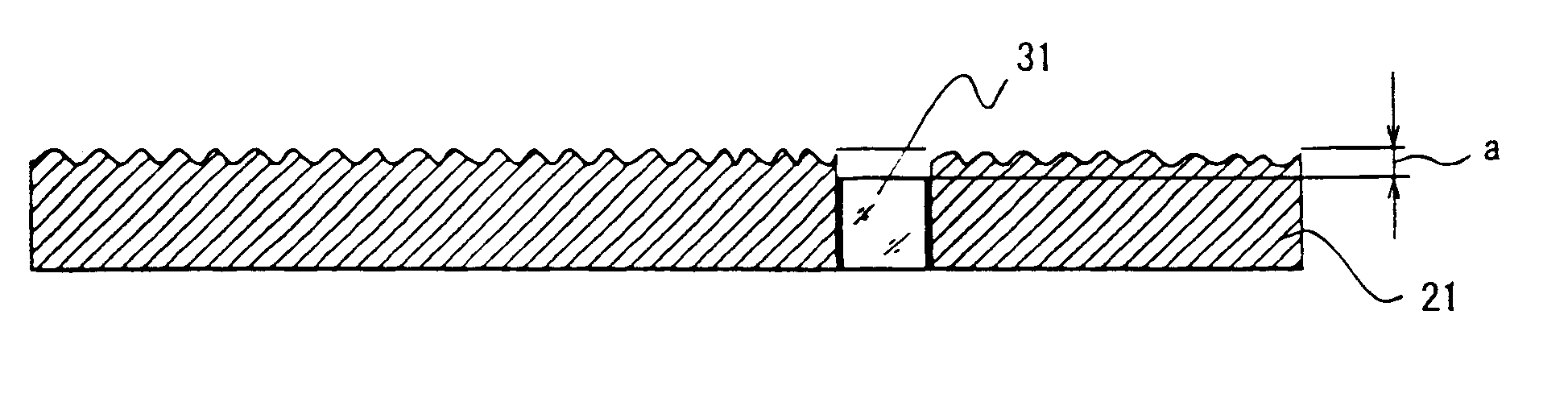
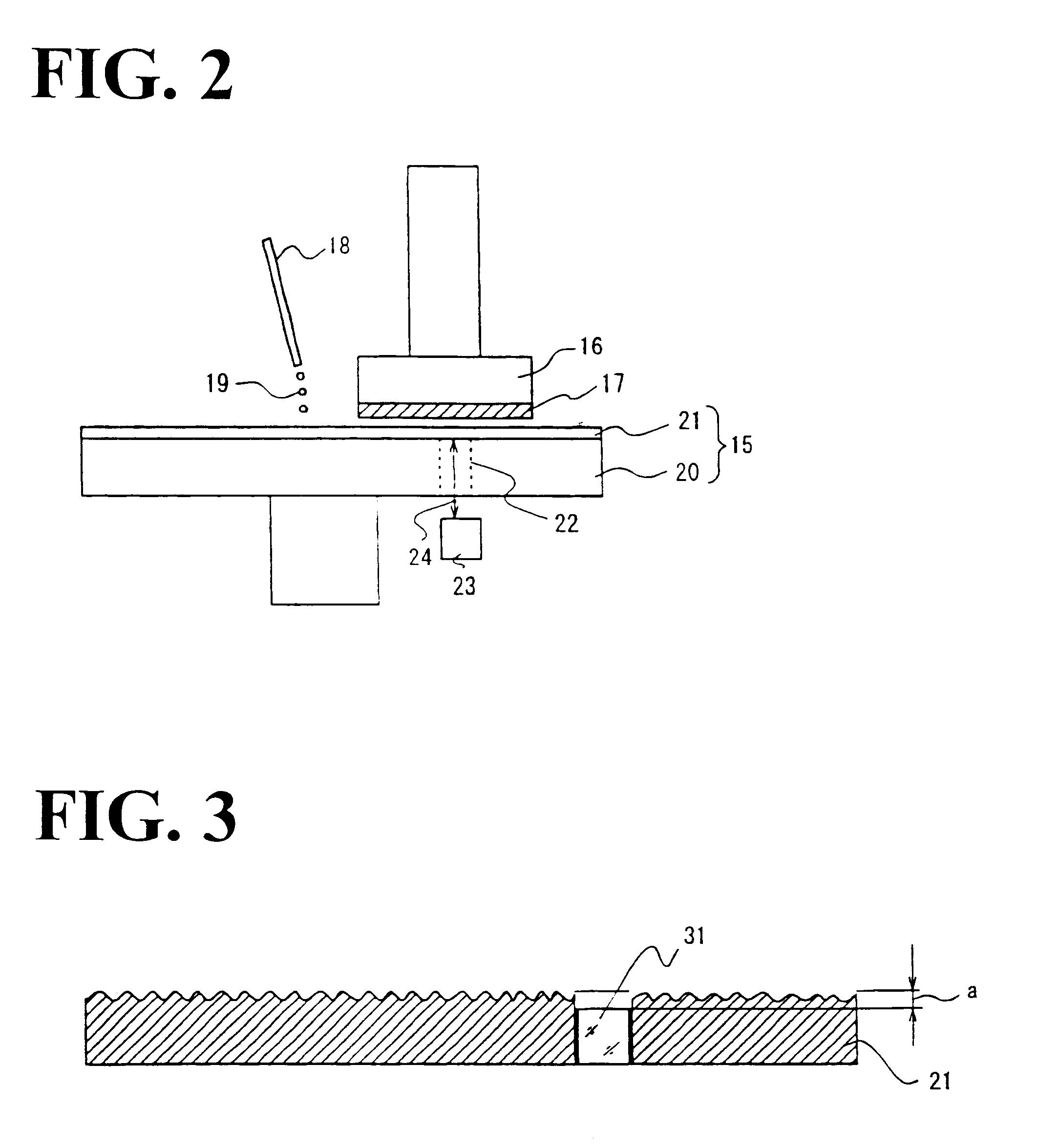
FIG. 4 is a diagram which is used to illustrate a second example of a polishing pad (polishing body) of the present invention. FIG. 4(a) is a plan view, FIG. 4(b) is a sectional view of the portion indicated by line A-O in FIG. 4(a), FIG. 4(c) is a sectional view of the portion indicated by line B-O in FIG. 4(a), and FIG. 4(d) is a sectional view of the portion indicated by line C-O in FIG. 4(a). In FIG. 4, 31a through 31c indicate window plates, and 32a through 32c indicate opening parts.

In the present example, the polishing body 21 has three opening parts 32a, 32b and 32c. Furthermore, a window plate 31a is disposed in the opening part 32a, a window plate 31b is disposed in the opening part 32b, and a window part 31c is disposed in the opening part 32c. In FIGS. 4(b), (c) and (d), the surface on the upper side of the polishing body 21 is the top surface of the polishing body 21, and the surfaces on the upper sides of the window plates 31a through 31c are the surfaces of the window...

example 1-3

FIG. 5 is a diagram which is used to illustrate a third example of a polishing pad (polishing body) of the present invention. FIG. 5(a) is a plan view, and FIG. 5(b) is a sectional view of the portion indicated by line D-E in FIG. 5(a). In FIG. 5, 32 indicates an opening part, and 33a through 33c indicate respective parts of a window plate 31.

The polishing body 21 of the present example has a single opening part 32. The window plate 31 disposed in this opening part 32 has a step-form cross section, so that the amount of recess of the surface of the window plate 31 on the side of the object of polishing with respect to the surface of the polishing body 21 differs in the three parts 33a, 33b and 33c. The amount of recess of the surface of the window plate 31 on the side of the object of polishing with respect to the surface of the polishing body 21 is smallest in the part 33a, and largest in the part 33c. In the part 33b, this amount of recess is more or less intermediate between that...

example 1-4

FIG. 6 is a diagram which is used to illustrate a fourth example of a polishing pad (polishing body) of the present invention. FIG. 6(a) is a plan view, and FIG. 6(b) is a sectional view of the portion indicated by line F-G in FIG. 6(a). In FIG. 6, 34a through 34d are points on the surface of the window plate 31.

The polishing body 21 of the present example has a single opening part. The parallel flat-plate window plate 31 installed in this opening part is devised so that it is inclined in section, with the amount of recess from the surface of the polishing body varying in the F-G direction in FIG. 6(a). As a result, the amount of recess of the surface of the window plate 31 on the side of the object of polishing varies in a continuous manner. In a case where four places 34a, 34b, 34c and 34d are designated on the surface of the window plate 31, the amount of recess of the surface of the window on the side of the object of polishing with respect to the surface of the polishing body i...


PUM

PropertyMeasurementUnit
thicknessaaaaaaaaaa
thicknesses t1aaaaaaaaaa
diameteraaaaaaaaaa

Abstract

After a hole is formed in a polishing pad, a transparent window plate is inserted into the hole. Here, a gap is left between the upper surface of the transparent window plate and the outermost surface constituting the working surface of the polishing pad. During polishing, the polishing head holding the wafer applies a load to the polishing pad by means of a load-applying mechanism, so that the polishing pad and transparent window plate are compressed. In this case, the system is arranged so that the gap remains constant, and so that a dimension equal to or greater than a standard value is maintained. Since the upper surface of the transparent window plate is recessed from the upper surface of the polishing pad, there is no scratching of the surface of the transparent window plate during dressing. Accordingly, the polishing pad has a long useful life.

Description

1. Field of the InventionThe present invention relates to a polishing body, polishing apparatus, polishing apparatus adjustment method and polished film thickness or polishing endpoint measurement method which are suitable for use in the polishing of semiconductor devices in a method for manufacturing semiconductor devices such as ULSI devices, etc., and to a semiconductor device manufacturing method.2. Discussion of the Related ArtAs semiconductor integrated circuits have become finer and more highly integrated, the individual processes involved in semiconductor manufacturing processes have become more numerous and complicated. However, the surfaces of semiconductor devices are not always flat. The presence of step differences on the surfaces of semiconductor devices leads to step breakage of wiring and local increases in resistance, etc., and thus causes wiring interruptions and drops in electrical capacitance. Furthermore, in insulating films such step differences also lead to a ...

Claims


Application Information

Patent Timeline
Patent Type & Authority Patents(United States)
IPC IPC(8): B24D7/12B24D7/00B24B37/04B24B49/04B24B49/02B24B49/12B24B37/013B24B37/20
CPCB24B37/013B24B37/205B24B49/04B24B49/12H01L21/304
Inventor IHSIKAWA, AKIRASENGA, TATSUYAMIYAJI, AKIRAUSHIO, YOSHIJIRO
Owner NIKON CORP
Why Eureka
Try Eureka