Plasma processing system for sputter deposition applications

a processing system and sputter technology, applied in the direction of vacuum evaporation coating, coating, electric discharge lamps, etc., can solve the problems of sub-micro scale elements on the substrate, localized charge buildup on the substrate surface, and non-uniform plasma generated with the configuration given in fig. 12

Inactive Publication Date: 2002-10-08
ANELVA CORP
View PDF2 Cites 89 Cited by
  • Summary
  • Abstract
  • Description
  • Claims
  • Application Information

AI Technical Summary

Problems solved by technology

However, the plasma generated with the configuration given in FIG. 12 is radially non-uniform.
This may cause localized charge build up on the substrate surface, specially if the substrate 112 is negatively biased by applying the rf electric power to the lower electrode 104, which eventually results in electrical breakdown of sub-micro scale elements on the substrate 107.

Method used


Image

  • Plasma processing system for sputter deposition applications
  • Plasma processing system for sputter deposition applications
  • Plasma processing system for sputter deposition applications

Examples


first embodiment

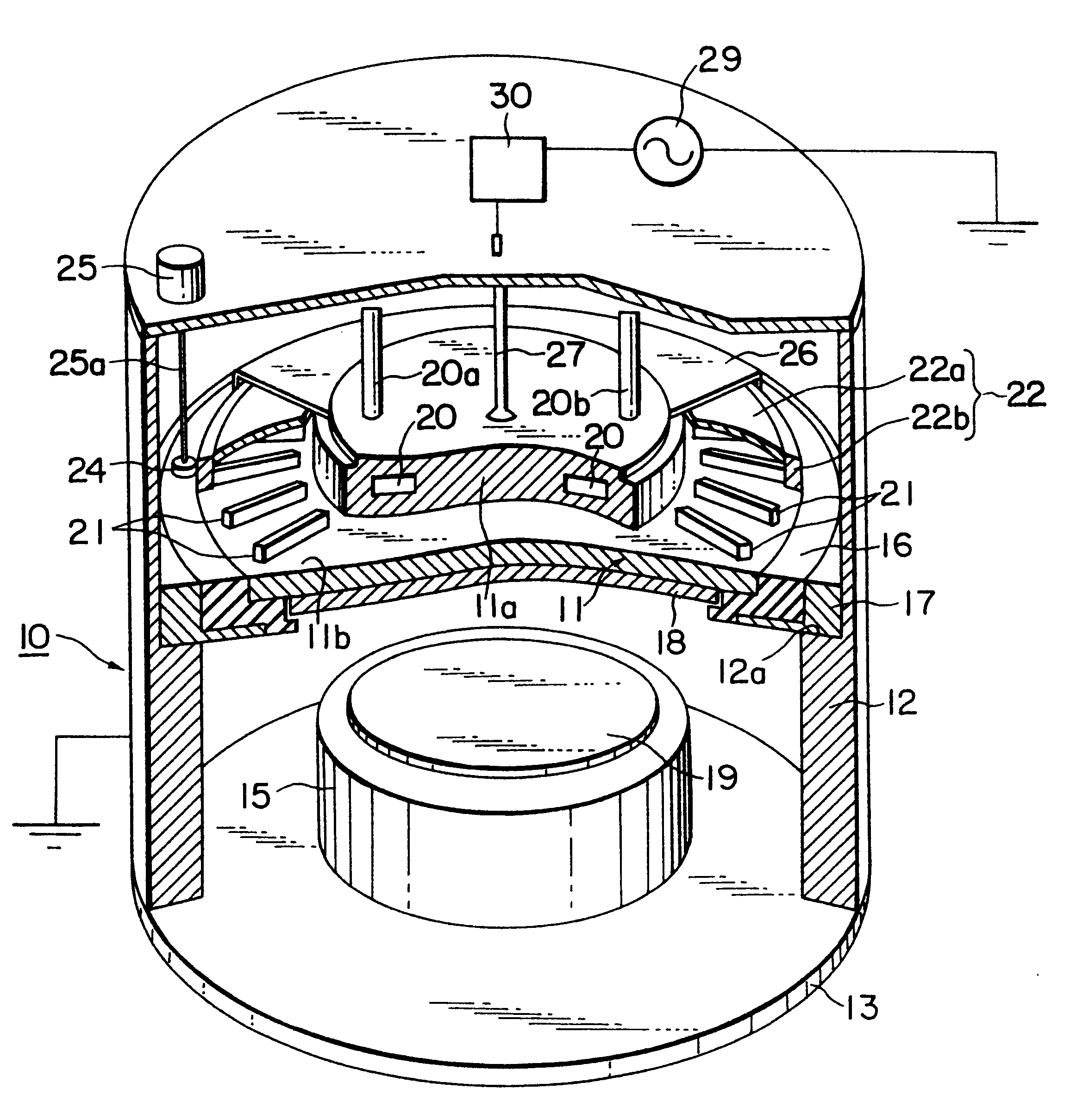
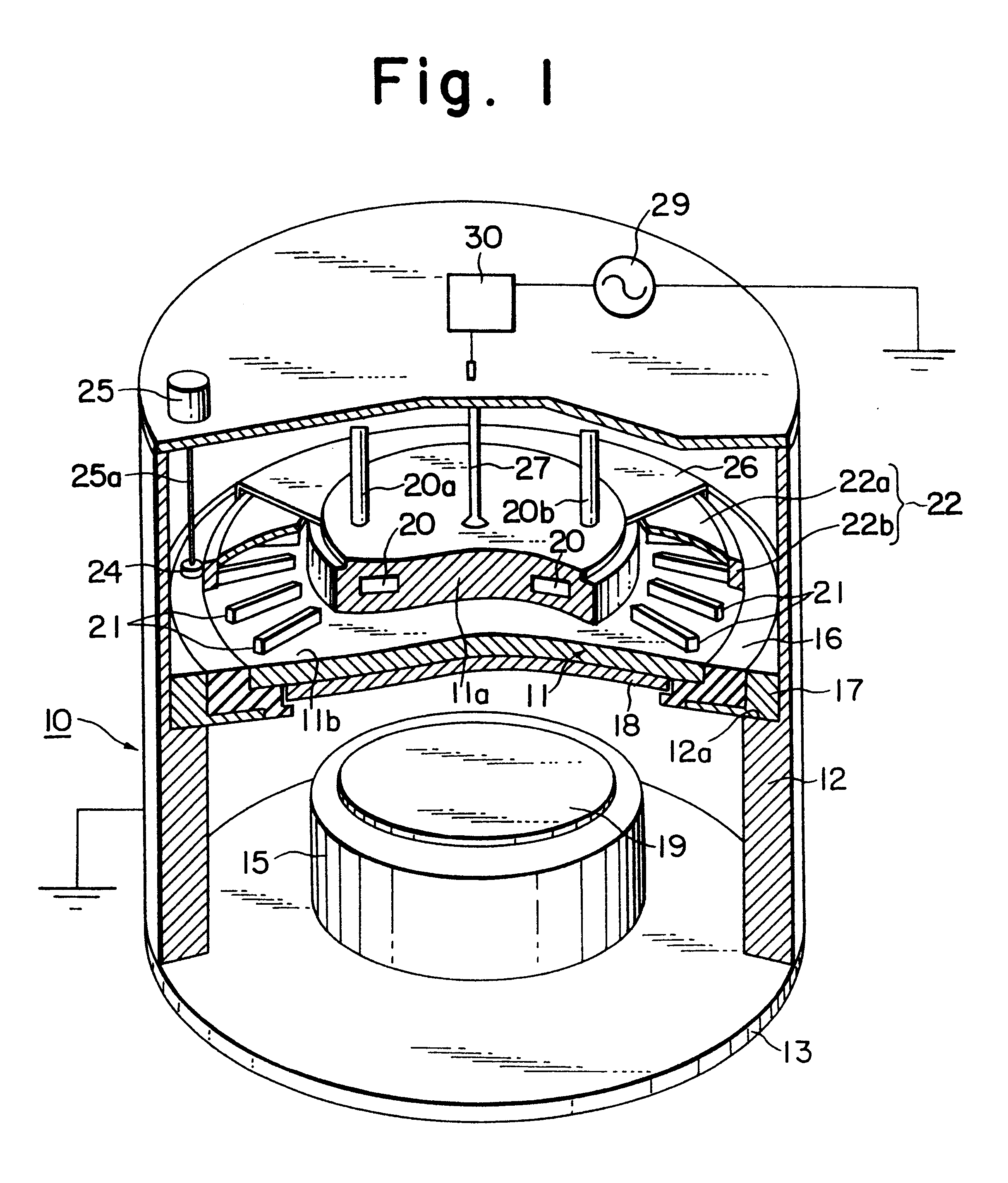
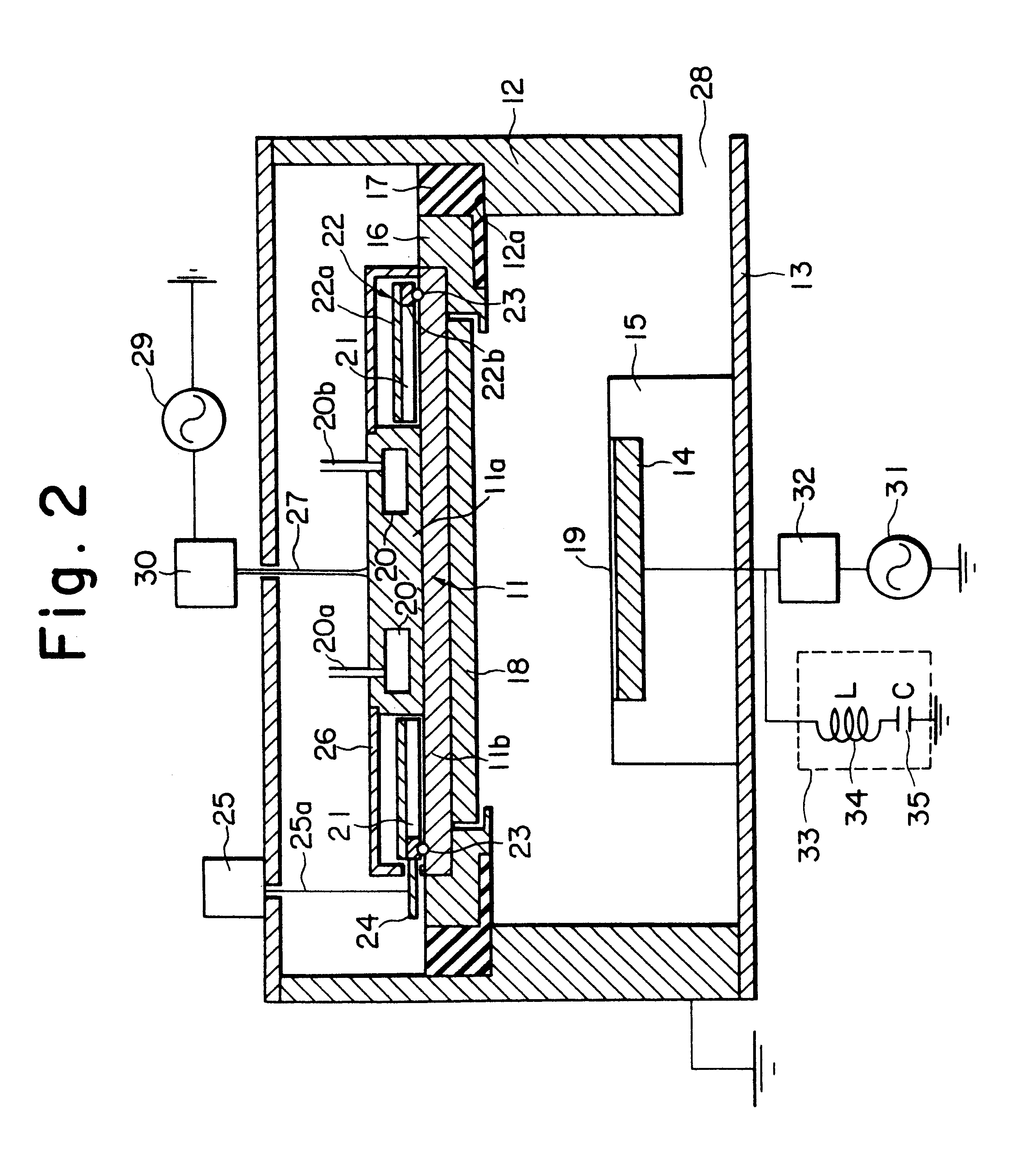
the present invention will be explained in accordance with FIGS. 1 and 2. FIGS. 1 and 2 show views of a plasma source used for a plasma processing system of the first embodiment. In this plasma processing system, 10 designates a reactor, 11 designates an upper electrode, 12 designates a cylindrical sidewall, 13 designates a bottom plate, 14 designates a lower electrode, and 15 designates a substrate holder. The upper electrode 11 is made of a non-magnetic metal, for example, Al, and placed on a ring 16 made of a dielectric material, for example, ceramic. The upper electrode 11 is of a circular shape. The dimensions of the upper electrode 11 are not critical and depend on the size of a substrate to be processed. The cylindrical side wall 12 and the bottom plate 13 are both made of a metal and electrically grounded.

The dielectric ring 16 is supported by a ring metal supporter 17 which is arranged on an inside step section 12a of the side wall 12. A target plate 18 of a round shape is ...

fifth embodiment

Next, the present invention is explained in accordance with FIG. 9. The hardware configuration of this embodiment is the same as that of the above-mentioned embodiments. This embodiment also has a special feature in the respect of the magnetic arrangement above the upper electrode. Therefore, FIG. 9 shows only the magnetic arrangement.

Many magnets 71 are arranged on the corners of hypothetical squares 72 with alternate polarity. The outer diameter of the magnetic arrangement region 73 is approximately equal to the diameter of the upper electrode 11. The magnets 71 are placed only within the region covered by radii r1 and r2 as shown in FIG. 9. The diameter and height of the magnet 71 are not critical. The diameter may lie in the range of 5 mm to 30 mm and the height may vary from 4 mm to 30 mm. The separation between two magnets 71 is also not critical and can be changed in the range of 15 mm to 40 mm. The plurality of magnets 71 are fixed to the above-mentioned metal ring 22 and ro...


PUM

PropertyMeasurementUnit
frequencyaaaaaaaaaa
thicknessaaaaaaaaaa
rotation frequencyaaaaaaaaaa

Abstract

A plasma processing system for sputter deposition application is configured by a reactor including two parallel capacitively-coupled electrodes called upper and lower electrodes, and a multi-pole magnet arrangement over the outer region of the upper electrode. The magnets are assembled on a metal ring in order to rotate over the upper electrode. The target plate is fixed to the upper electrode which is given only a high-frequency rf current, or high-frequency rf current and a DC voltage together. The lower electrode where the substrate is placed, is given a MF, HF or VHF rf current in order to generate a negative self bias voltage on the lower electrode to extract ionized sputtered-atoms that fill contact-holes on the substrate surface.

Description

1. Field of the InventionThe present invention relates to a plasma processing system for sputter deposition applications, and more particularly, to a plasma processing system like a plasma assisted sputtering system having an improved plasma source capable of independently controlling plasma ion density and ion energy at the rf (high-frequency AC) electrodes useful for a sputtering process of metal or dielectric materials during the fabrication of integrated circuits in the semiconductor industry.2. Description of the Related ArtLarge-area and high-density plasma sources with higher radial uniformity are of great demand to process large area substrates without charge-induced damages to the devices fabricated on the substrate surface. Specially, development of new plasma sources for the sputtering process of metal and dielectric materials with enhanced uniformity of the deposited film is of important. Difficulties in obtaining the above-mentioned properties with conventional plasma s...

Claims


Application Information

Patent Timeline
Patent Type & Authority Patents(United States)
IPC IPC(8): C23C14/35H01J37/32H01J37/34H01L21/205
CPCC23C14/35H01J37/32165H01J37/3402H01J37/3452H01J37/3455
Inventor WICKRAMANAYAKA, SUNILNAKAGAWA, YUKITO
Owner ANELVA CORP
Why Eureka
Try Eureka