Supercharge Your Innovation With Domain-Expert AI Agents!

Screening of semiconductor integrated circuit devices

a technology of integrated circuit devices and semiconductors, applied in the testing of individual semiconductor devices, measurement devices, instruments, etc., can solve the problems of long time, hundreds or thousands of hours to complete the test, and obvious temperature-dependent potential failures in a relatively short period of tim

Inactive Publication Date: 2002-11-12
RENESAS ELECTRONICS CORP
View PDF4 Cites 0 Cited by
  • Summary
  • Abstract
  • Description
  • Claims
  • Application Information

AI Technical Summary

Benefits of technology

Still another object of the present invention is to provide a method of screening semiconductor integrated circuit devices that screens out faulty devices with potential failure in a short period of time, and a computer program product that performs the method.
A further object of the present invention is to provide an apparatus for screening semiconductor integrated circuit devices capable of screening out faulty devices with potential failure in a short period of time.
Moreover, since no burn-in test is necessary, faulty devices with potential failure can be screened out in a short period of time.
In a preferred embodiment of the method according to the first aspect, further comprising a step of performing a burn-in test for the devices prior to the step (a). In this embodiment, there is an additional advantage that faulty devices can be screened out more accurately than the case where no burn-in test is carried out prior to the step (a).

Problems solved by technology

This is a method to deliberately apply electrical stress to LSIs to be tested in a high-temperature environment, thereby making temperature-dependent potential failures obvious in a comparatively short period of time.
However, this test has a disadvantage that it may take a long time such as several hundreds or several thousands hours to complete the test when the type of failure modes to be elicited is time-consuming and / or the required level of reliability is high.
Moreover, the burn-in test has a danger that the potential failure of LSIs is unable to be found or observed, which is due to the following reason.
Specifically,. potential defects or failures existing in LSIs degrade gradually with time due to applied stresses in the burn-in test.
Thus, there is a possibility that the potential defects or failures in LSIs are not found even if the test is finished.
Thus, when the distribution of the set of power spectrum data of the power supply current of one of the devices is equal to or greater than the reference value, the device in question is regarded as a faulty or good one.
As a result, faulty devices can be screened out before potential failure existing therein through a burn-in test is elicited.
Moreover, since no burn-in test is necessary, faulty devices with potential failure can be screened out in a short period of time.
In contrast, the faulty devices have large change rates of the power spectrum data, because the faulty devices include some potential fault or defect and therefore, they distinctly degrade in performance after the burn-in test is completed.

Method used


Image

  • Screening of semiconductor integrated circuit devices
  • Screening of semiconductor integrated circuit devices
  • Screening of semiconductor integrated circuit devices

Examples


first embodiment

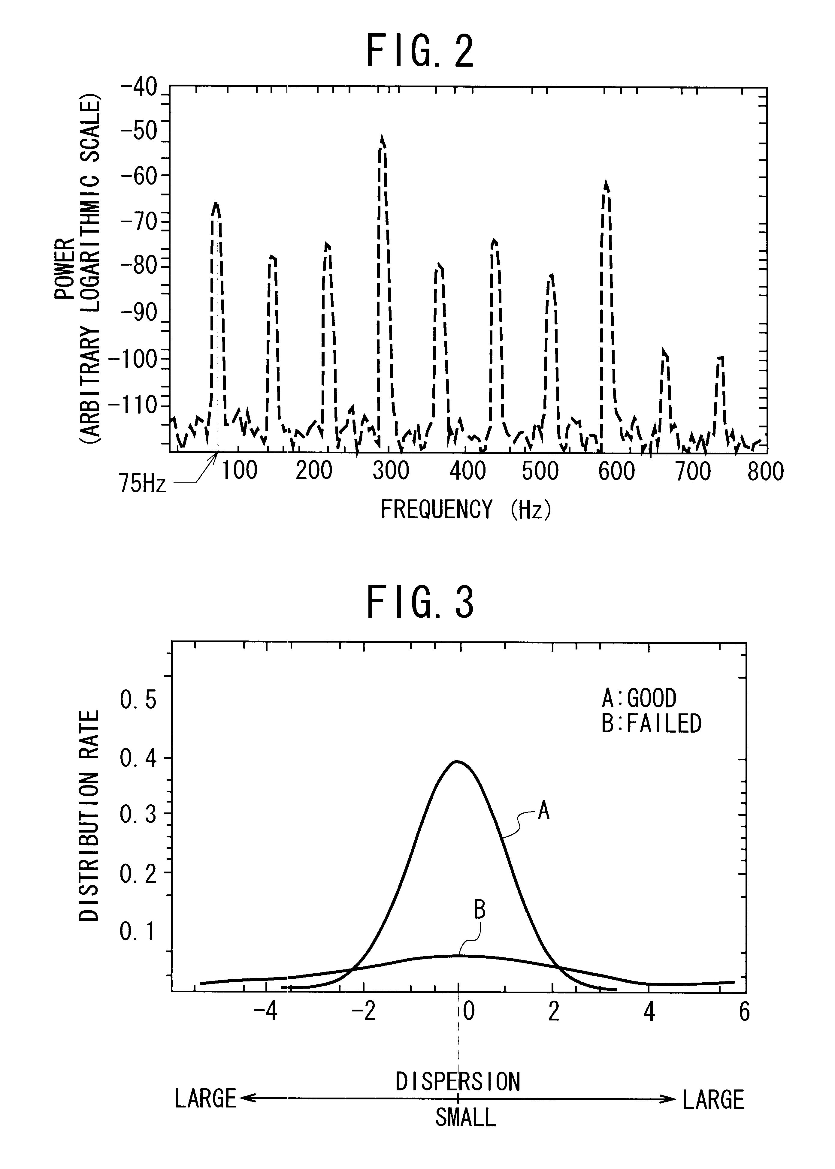
Next, prior to explanation of the screening method the principle of the method is explained below with reference to FIGS. 2 and 3.

FIG. 2 shows an example of the power spectrum of the power supply current flowing into one of the DUTs or LSIs 4, which was obtained by applying repeatedly the test signal S.sub.TEST to the respective DUTs 4 while the period T of the test signal S.sub.TEST (which includes a set of test patterns) was set as 13.3 milliseconds (ms) (i.e., T=13.3 ms). FIG. 3 shows an example of the distribution rate change as a function of dispersion of the power spectrum data D.sub.SPEC of one of the power supply currents.

The power supply current flowing into each of the DUTs 4 contains a lot of information reflecting the internal state of the DUT 4 serving as a load. In other words, if one of the DUTs 4 has a defect that leads to early failure (e.g., defective interconnections or wiring lines, defective transistors, and so on), the power supply current flows abnormally int...

second embodiment

FIG. 7 is a flowchart showing the steps of a screening method according to a second embodiment of the invention, which is carried out by the screening apparatus according to the first embodiment of FIG. 1.

As seen from FIG. 7, the method of the second embodiment comprises a step S11 of performing a burn-in test and a step S12 of performing the screening procedure (i.e., the steps S1 to S6 in FIG. 4). In other words, the method of the second embodiment is the combination of a burn-in test and the steps S1 to S6 in the screening method according to the first embodiment.

Thus, with the screening method of the second embodiment, a burn-in test is carried out in a short period of time before the screening procedure (i.e., S1 to S6) and therefore, the potential faulty existing in the DUTs 4 tend to be elicited prior to the procedure As a result, there is an additional advantage that the faulty LSIs or DUTs 4 with potential failure therein can be screened out at a higher accuracy than the me...

third embodiment

FIG. 8 is a flowchart showing the steps of a screening method according to a third embodiment of the invention, which is carried out by the screening apparatus according to the first embodiment of FIG. 1.

As seen from FIG. 8, the method of the third embodiment comprises a step S21 of performing the screening procedure (i.e., the steps S1 to 96 in FIG. 4), a step S22 of performing the screening procedure (i.e., the steps S1 to S6 in FIG. 4) during a burn-in test, and a step S23 of performing the screening procedure (i.e., the steps S1 to S6 in FIG. 4). In other words, the steps S1 to S6 in the screening method according to the first embodiment are carried out (the first time) in the step S21 before a burn-in test is started, the same steps S1 to S6 are carried out (the second time) during the burn-in test in the step S22, and the same steps S1 to S6 are carried out (the third time) in the step S23 after the burn-in test is completed.

Specifically, with the screening method of the third...


PUM


Abstract

A method of screening LSIs is provided, which makes it possible to screen out faulty LSIs before potential failure existing therein is elicited. A specific power supply voltage is supplied to LSIs to be tested while applying a specific test signal to the LSIs at a specific period. Power supply currents of the LSIs are observed. Sets of power spectrum data of the power supply currents are generated corresponding to the test signal. The distributions of the sets of power spectrum data are generated. whether or not the distributions of the sets of power spectrum data of the power supply currents are equal to or greater than a specific reference value is judged. When the distribution of the set of power spectrum data of the power supply current of one of the devices is equal is to or greater than the reference value, the device in question is regarded as a faulty one.

Description

1. Field of the InventionThe present invention relates to a screening technique of semiconductor integrated circuit devices, e.g., Large-Scale Integrated circuit devices (LSIs). More particularly, the invention relates to a method of and an apparatus for screening semiconductor integrated circuit devices that screen out faulty devices (i.e., LSIs with some early failure), and a computer program product having a computer readable medium and a computer program recorded thereon that performs the method.2. Description of the Related ArtConventionally, the "burn-in" test or procedure has been well known and actually performed as a method of screening out defective LSIs with some early failure. This test or procedure is explained in detail, for example, in a book entitled "Integrated Circuit Quality and Reliability" written by Eugene R. Hnatek, pp. 719-720. This is a method to deliberately apply electrical stress to LSIs to be tested in a high-temperature environment, thereby making tempe...

Claims


Application Information

Patent Timeline
Patent Type & Authority Patents(United States)
IPC IPC(8): G01R31/319G01R31/28G01R31/26G06F9/44
CPCG01R31/319G06F8/00
Inventor SAKAGUCHI, KAZUHIRO
Owner RENESAS ELECTRONICS CORP
Features
  • R&D
  • Intellectual Property
  • Life Sciences
  • Materials
  • Tech Scout
  • Unparalleled Data Quality
  • Higher Quality Content
  • 60% Fewer Hallucinations
Learn More