Semiconductor wafer having regular or irregular chip pattern and dicing method for the same

a technology of semiconductor wafers and chip patterns, applied in the field of semiconductor wafers, can solve the problems of significant amount of remaining material left to be discarded, difficult to avoid the waste of semiconductor materials,

Inactive Publication Date: 2003-03-04
DISCO CORP
View PDF3 Cites 180 Cited by
  • Summary
  • Abstract
  • Description
  • Claims
  • Application Information

AI Technical Summary

Problems solved by technology

Also disadvantageously, use of the dicing machine makes it difficult to avoid the waste of sem...

Method used


Image

  • Semiconductor wafer having regular or irregular chip pattern and dicing method for the same
  • Semiconductor wafer having regular or irregular chip pattern and dicing method for the same
  • Semiconductor wafer having regular or irregular chip pattern and dicing method for the same

Examples


second embodiment

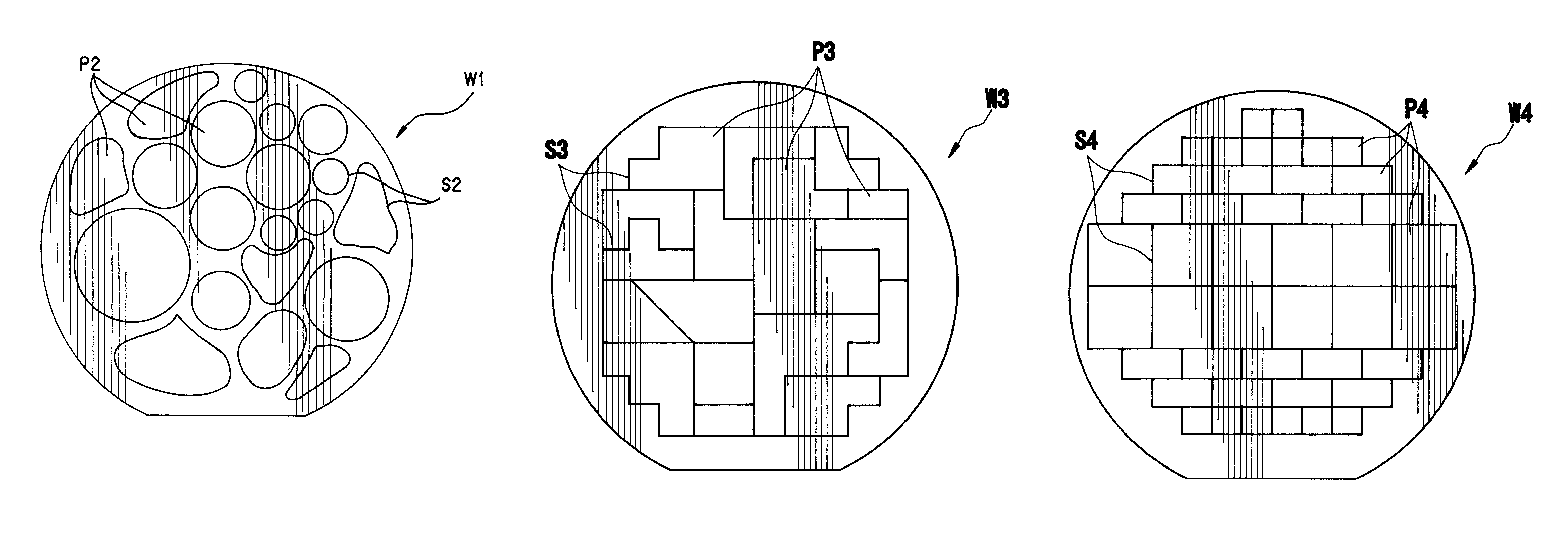
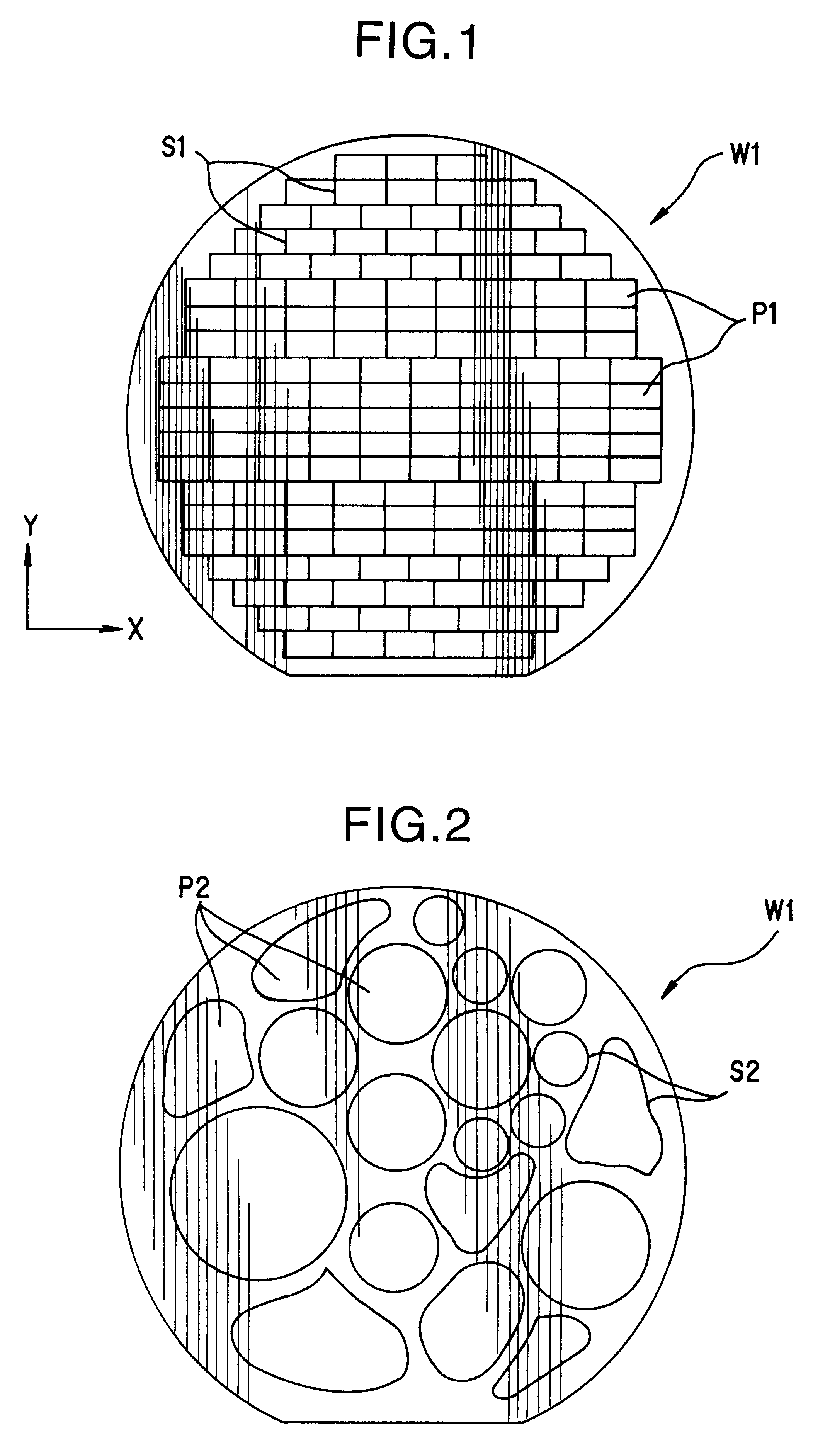
Referring to FIG. 2, a semiconductor wafer W2 has a plurality of chip areas P2 of circles and irregular curved shapes formed thereon. These chip areas P2 have streets S2 running therebetween.

third embodiment

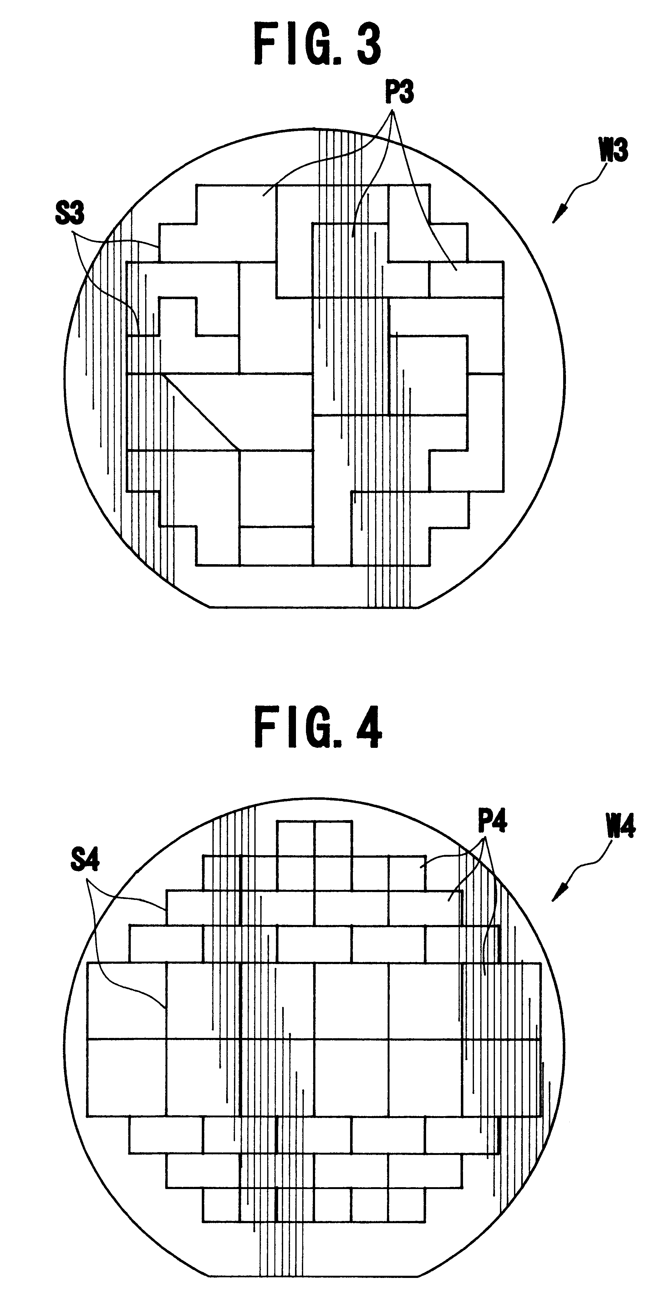
Referring to FIG. 3, a semiconductor wafer W3 has a plurality of chip areas P3 of rectangular and irregular polygonal shapes formed thereon. These chip areas P3 have streets S3 running therebetween.

fourth embodiment

Referring to FIG. 4, a semiconductor wafer W4 has a plurality of chip areas P4 of rectangular and square shapes of different sizes arranged closely to each other. These chip areas P4 have line segment streets S4 running therebetween. As is the case with the staggered-lattice pattern as shown in FIG. 1, the longitudinal streets S4 of sub-arrangements of chip areas are staggered laterally in the X-axial direction. The lateral streets of the sub-arrangement of square chip areas are separated a distance twice as long as that in each sub-arrangement of rectangular chip areas in the Y-axial direction.

As seen from FIGS. 1 to 4, in every semiconductor wafer chip areas are so arranged as to make full use of the whole area of the semiconductor wafer, minimizing the waste of semiconductor material. Thus, the number of chips per wafer can be increased 5 to 10 or more percent.

Chip areas of different sizes and shapes can be formed on semiconductor wafer by transferring desired shapes thereon wit...


PUM


Abstract

Disclosed is a semiconductor wafer whose pattern is composed of a plurality of chip areas delimited by a plurality of streets which at least one or more streets are not straight. Those chip areas may be rectangular ones of same or different sizes delimited by streets which are wholly or partly staggered, or ones of different shapes and/or sizes delimited by streets which are bent or curved so that they may separate adjacent chip areas. Such a semiconductor wafer can be separated into chips by: coating one of the opposite surfaces of each semiconductor wafer with a photo-resistive film; exposing the coated surface of the semiconductor wafer to the light to remove the coating area lying on the streets; subjecting the street-exposed wafer surface to chemical etching to make grooves in conformity with the streets; and separating the semiconductor wafer into chips. The separating step may include making grooves deep enough to reach the front side of the wafer by chemical etching or grinding the grooved wafer on its rear side to remove the remaining thickness of the grooved wafer.

Description

1. Field of the InventionThe present invention relates to a semiconductor wafer to be diced into semiconductor chips of same or different shapes for making the best use of semiconductor materials and sizes and a method of dicing such a semiconductor wafer.2. Related ArtsReferring to FIG. 12, a semiconductor wafer W has a lattice pattern formed therein, delimiting a plurality of chip areas P of same size by crossing streets S. The semiconductor wafer W can be cut and divided into separate chips P by a dicing machine.Use of such a dicing machine requires crosswise arrangement of straight streets S, thus preventing the cutting of a semiconductor wafer into chips of different shapes and / or sizes, such as circle, trapezoid, "L"-shape, concave or convex shape. Also disadvantageously, use of the dicing machine makes it difficult to avoid the waste of semiconductor material, allowing a significant amount of remaining material to be left and thrown away.One object of the present invention is...

Claims


Application Information

Patent Timeline
IPC IPC(8): H01L21/02H01L21/00H01L21/304H01L21/70H01L21/78H01L21/301
CPCH01L21/3043H01L21/6715H01L21/67092H01L21/78H01L21/30
Inventor ARAI, KAZUHISA
Owner DISCO CORP
Why Eureka
Try Eureka