
Planar filter and filter system using a magnetic tuning member to provide permittivity adjustment

a filter system and magnetic tuning technology, applied in the field of planar filters, can solve the problems of large change in resonance properties, inability to obtain desired filter properties, and high degree of accuracy in adjusting resonance properties

Inactive Publication Date: 2003-03-11
KK TOSHIBA
View PDF5 Cites 10 Cited by
  • Summary
  • Abstract
  • Description
  • Claims
  • Application Information

AI Technical Summary

Benefits of technology

Further object of the present invention is to provide a planar filter which can tune a pass frequency band at a high speed and in a broad range with a simple constitution without sacrificing a low loss property of a superconductor.
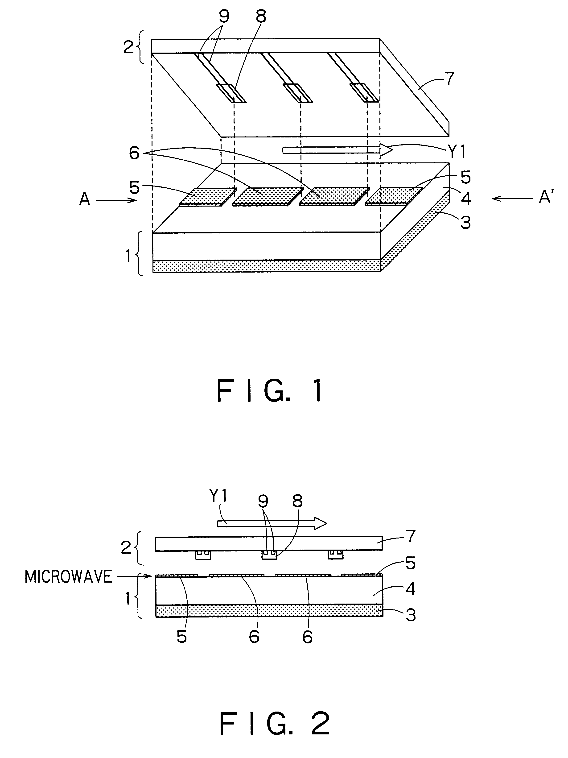
According to the present invention, the filter member is disposed opposite to the tuning member, and the tuning member can adjust the effective permittivity of at least one of the gap periphery between the resonance elements in the filter member, and the gap periphery between the input / output portion and the resonance element. Because of this, when changing the filter pass frequency band, the skirt property can be improved, and the ripple can be eliminated.
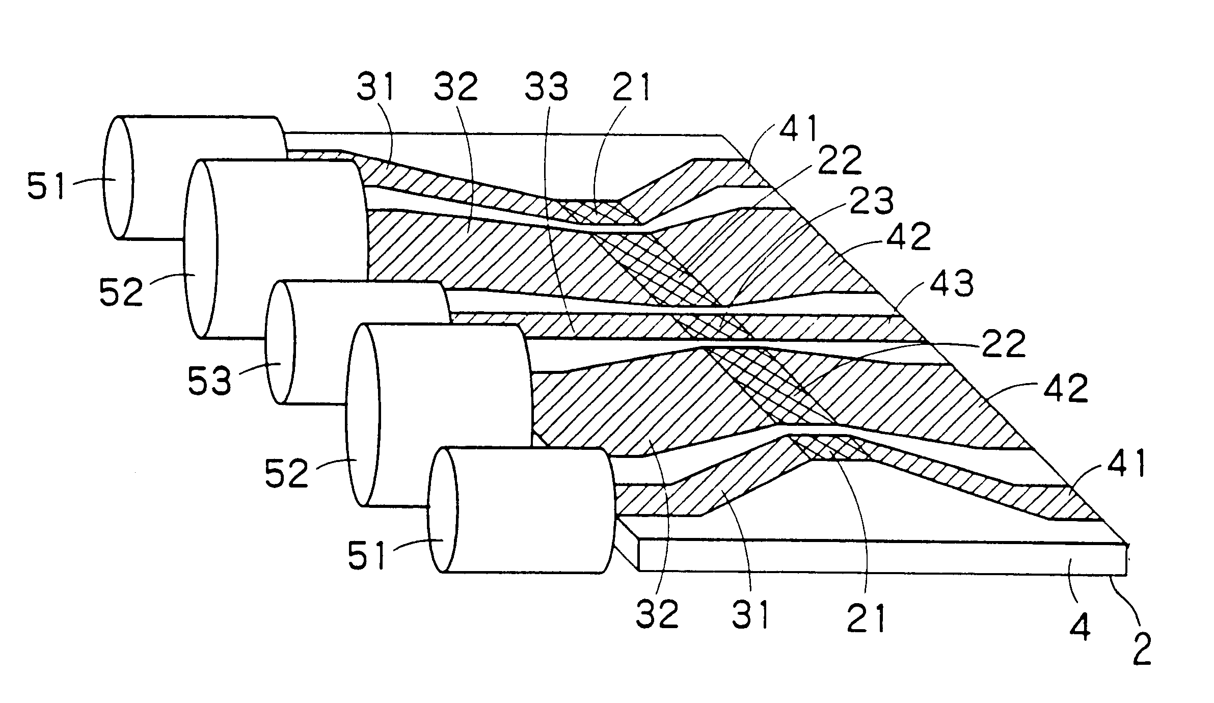
According to the present invention, by disposing the tuning member including the first to third magnetic materials opposite to the filter member, and adjusting the permeability of the first to third magnetic materials, the resonance frequency, the coupling between the resonance elements, and the coupling between the resonance element and the input / output portion can variably be controlled, and the skirt property, ripple, and other filter properties can be improved.

Problems solved by technology

On the other hand, there is a problem that the resonance property has to be adjusted with a high degree of accuracy when designing and making the filter.
That is, by a slight dispersion of permittivity of the substrate or a slight processing error of the conductor during processing, the resonance property largely changes, and a desired filter property cannot be obtained.
Moreover, even when the desired filter property is obtained, there is also a problem that a deviation is generated in the filter property of variation with time or ambient temperature change.
However, in a conventional technique, the dielectric for changing the permittivity, and the electrode for applying the voltage are essential constituting elements, losses by the dielectric and electrode lowers the Q value of the resonance element down to several hundreds or less, and it is difficult to obtain the resonance element and filter superior in attenuation property and small in insertion loss.
However, when this technique is applied to tune the filter property, only the uniform magnetic field can be applied to the respective resonance elements and between the resonance elements or to the input / output portion, the individual and independent adjustments of the aforementioned adjustments (1) to (3), necessary for tuning the filter pass frequency band, are therefore impossible, and there is a problem that changing of the pass frequency band deteriorates the skirt property and ripple.

Method used


Image

  • Planar filter and filter system using a magnetic tuning member to provide permittivity adjustment
  • Planar filter and filter system using a magnetic tuning member to provide permittivity adjustment
  • Planar filter and filter system using a magnetic tuning member to provide permittivity adjustment

Examples


first embodiment

first concrete example described hereinafter is a concrete example of the filter of FIG. 1 described in the first embodiment, and a band pass filter of a micro-strip line structure of a 4.8 GHz band will be described.

In the present example, 0.5 mm thick LaAlO, was used as the substrate 4 of the filter member 1. A yttrium-based superconductor thin film was formed in 500 nm on both surfaces of the substrate 4 by a sputtering method, the superconductor thin film on one surface was used as the ground surface 3, the superconductor thin film of the other surface was processed using an ion milling method, the input / output portion 5 and a plurality of resonance elements 6 with a desired resonance frequency were formed, and the filter member 1 of the micro-strip line structure was prepared.

Each resonance element 6 obtained a width of 170 .mu.m, length of 8 mm, and resonance frequency of 4.8 GHz. Moreover, a 100 .mu.m gap was disposed between the resonance elements 6, and a 70 .mu.m gap was d...

second concrete example

A second concrete example described hereinafter is, similarly as the first concrete example, a concrete example of the first embodiment, and an example with a pass frequency band of about 2 GHz is shown.

FIGS. 11A-11C are views showing a structure of the second concrete example of the planar filter. FIG. 11A is a plan view of the filter member 1, FIG. 11B is a plan view of the tuning member 2, and FIG. 11C is a sectional view of the planar filter.

The planar filter of FIGS. 11A and 11C are similar in structure and manufacture method to the planar filter of FIG. 1, except that the shape of the resonance element 6 on the filter member 1 is different. Therefore, a detailed description of the elements shown in FIGS. 11A-11C has been provided with respect to FIG. 1 and is not repeated in relation to FIGS. 11A-11C.

As shown in the equation (1), when the resonance frequency is lowered, the length L of the resonance element 6 is lengthened. Therefore, in the filter member 1 of FIG. 11A, the re...

third concrete example

A third concrete example described hereinafter is a concrete example of the filter of FIGS. 4A and 4B described in the second embodiment.

In the third concrete example, the planar filter shown in FIGS. 4A and 4B was prepared in the following method. On both surfaces of the single-crystal substrate 4 of LaAlO.sub.3 with a longitudinal size of 40 mm, lateral size of 20 mm and thickness of 0.5 mm, a 500 nm thick YBCO superconductor film was formed by the sputtering method, laser vapor deposition method, CVD method, or the like. Next, one surface was processed by a lithography method to form the input / output portion 5 and resonance element 6, and then the back surface of the substrate was used as the ground surface 3 and a two-stage band pass filter of a micro-strip structure was prepared.

The width of the resonance element 6 was set to 170 .mu.m, the length thereof was 8 mm, the gap between the resonance elements 6 was 100 .mu.m, and the gap between the resonance element 6 and the input / ...


PUM

PropertyMeasurementUnit
thickaaaaaaaaaa
lengthaaaaaaaaaa
lengthaaaaaaaaaa

Abstract

There is disclosed a planar filter which can variably control a pass frequency band with a high precision and which is superior in skirt property and little in ripple. A planar filter member and tuning member are disposed opposite to each other via a predetermined gap. The filter member is structured in such a manner that an input / output portion formed of a superconductor and a plurality of resonance elements are formed on a substrate. The tuning member is structured in such a manner that on the surface of a magnetic plate with a permeability changing by an applied magnetic field, a plurality of dielectric thin films, and a plurality of electrodes for applying electric fields to the dielectric thin films are arranged. Each of the dielectric thin films is disposed in a position opposite to a gap between the resonance elements of the filter member, or a gap between the filter member and the input / output portion. By applying a voltage between the electrodes, an effective permittivity is in of the gap between the resonance elements, or the gap between the resonance element and the input / output portion is variably controlled, and the skirt property and ripple are adjusted. Moreover, a resonance frequency of the resonance elements, a coupling between the resonance elements, and a coupling between the resonance element and the input / output portion may be individually and independently controlled.

Description

The subject application is related to subject matter disclosed in Japanese Patent Application No. H11-276626 filed on Sep. 29, 1999 in Japan to which the subject application claims priority under Paris convention and which is incorporated herein by reference.1. Field of the InventionThe present invention relates to a planar filter constituted by disposing a filter member opposite to a tuning member, particularly to a technique of using a superconductor as a filter material for use in a communication apparatus and the like.2. Related Background ArtIn a communication apparatus for performing information communication by radio or cable, a filter for extracting only a desired frequency band is an important constituting component. To realize the effective use of a frequency, and energy savings, a filter superior in attenuation property and small in insertion loss is demanded.To satisfy such a demand, a resonance element high in a Q value is necessary as a filter constituting element. As ...

Claims


Application Information

Patent Timeline
Patent Type & Authority Patents(United States)
IPC IPC(8): H01P1/203H01P1/20
CPCH01P1/20363Y10S505/701Y10S505/866Y10S505/70H01P1/203
Inventor TERASHIMA, YOSHIAKIFUKE, HIROYUKIKAYANO, HIROYUKIYOSHINO, HISASHI
Owner KK TOSHIBA
Learn More