On-chip fixed-pattern noise calibration for CMOS image sensors

a technology of image sensor and fixed pattern, which is applied in the field of on-chip fixed pattern noise calibration of cmos image sensor, can solve the problems of variable memory unit cost increase, fixed pattern noise (fpn), and noise type generation in cmos image sensor technology

Inactive Publication Date: 2003-03-25
HANGER SOLUTIONS LLC
View PDF18 Cites 46 Cited by
  • Summary
  • Abstract
  • Description
  • Claims
  • Application Information

AI Technical Summary

Benefits of technology

An on-chip FPN calibration method and circuits scheme applies a reference voltage signal to an array of calibration pixels coupled to a sensor matrix. Two data values are read from each bit line and used to calculate an offset and a gain error for a pixel column, the offset being the first data value and the gain error being the slope of the first and second data value read for each bit line. A reference offset and a reference gain error value are then generated by computing the average offset and the average gain error from the collected offset

Problems solved by technology

However, a major drawback of the CMOS image sensor technology is the presence of fixed-pattern noise (FPN).
This type of noise is generated from a mismatch of circuit structures in the integrated circuits process variat

Method used


Image

  • On-chip fixed-pattern noise calibration for CMOS image sensors
  • On-chip fixed-pattern noise calibration for CMOS image sensors
  • On-chip fixed-pattern noise calibration for CMOS image sensors

Examples


Embodiment Construction

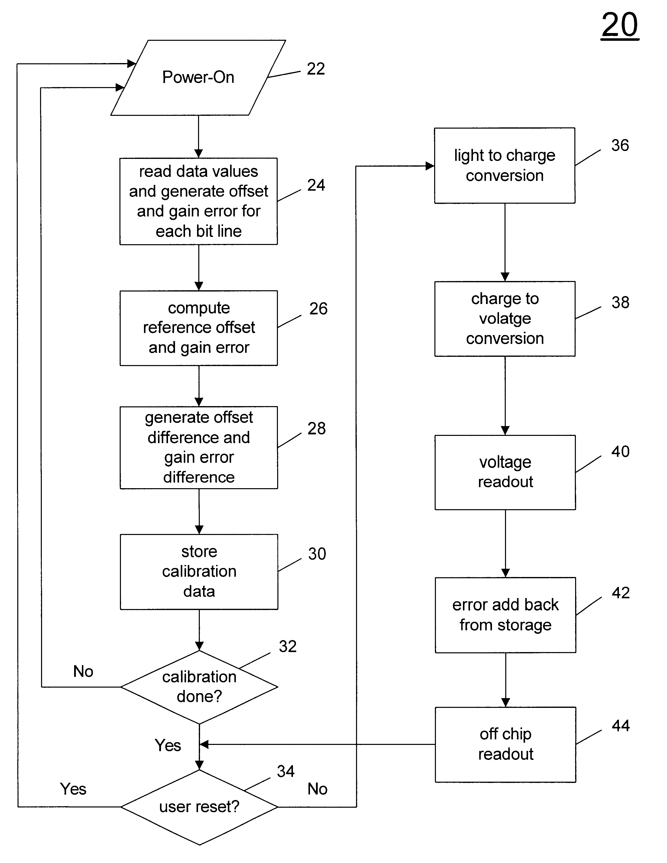
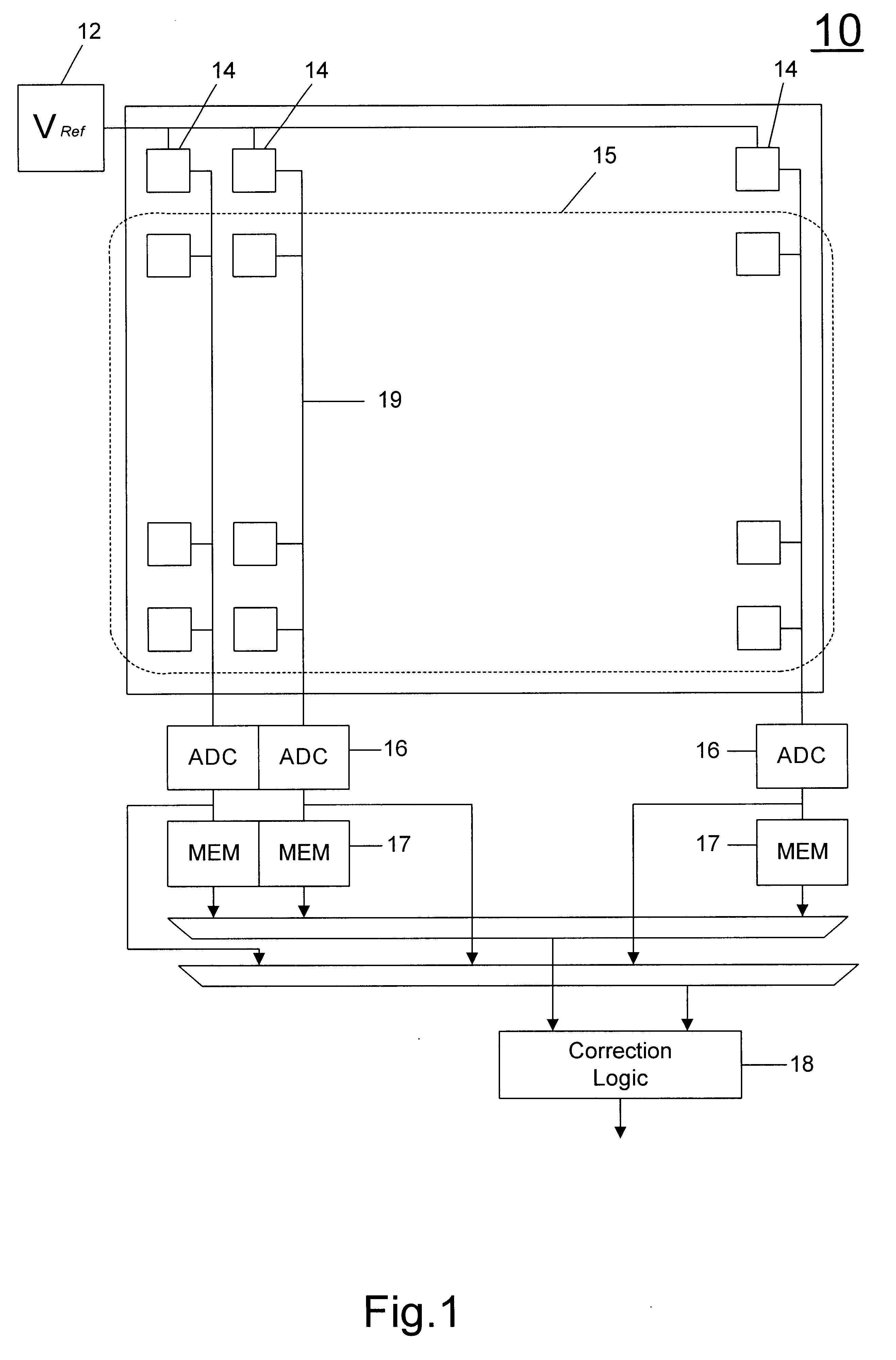
FIG. 1 illustrates a general system-level block diagram of an on-chip FPN calibration architecture 10 for CMOS image sensors designed in accordance with the principles of this invention. Calibration can be designed to be invoked either at power-on of an image sensor chip, at the activation of a reset signal (RS) at user's control, or otherwise, depending on desired design specifications. As illustrated in FIG. 1, a row of calibration pixel circuits 14 is added to a sensor matrix 15, a calibration pixel circuit 14 is provided for each array of pixels in matrix 15, such as for each column of pixels, wherein each pixel column is coupled to a pixel column output bit line 19. A reference voltage signal 12 (Vref) is applied as input to each calibration pixel 14.

During FPN calibration and correction process, two data values are read out of each calibration pixel 14 from each bit line 19 via ADC circuitry 16 and provided to correction logic 18. Correction logic 18 generates a corresponding ...


PUM


Abstract

An on-chip FPN calibration method and circuits scheme applying a reference voltage signal to an array of calibration pixels coupled to a sensor matrix. Two data values are read from each bit line and used to calculate an offset and a gain error for a pixel column. A reference offset and a reference gain error value are then generated by computing the average offset and the average gain error from the collected offset and gain error values of each bit line. Calibration data for each bit line then comprises an offset difference and a gain error difference, the offset difference comprising the difference between the offset value for that bit line and the reference offset, and the gain error difference comprising the gain error difference between the gain error for that bit line and the reference gain error. The calibration data for each bit line is then stored in on-chip volatile memory and is used later under normal operation to compensate for the FPN effect.

Description

The present invention relates to complementary metal oxide semiconductor image sensors, and more particularly, to methods for on-chip calibration and correction of fixed-pattern noise.BACKGROUND OF INVENTIONComplementary metal oxide semiconductor (CMOS) image sensor technology is poised to take over the existing CCD (charge-coupled-device) technology in the market of image and video capture. CMOS technology offers many benefits, such as lower cost, ease of manufacturing, and a higher degree of integration over the CCD. However, a major drawback of the CMOS image sensor technology is the presence of fixed-pattern noise (FPN). This type of noise is generated from a mismatch of circuit structures in the integrated circuits process variations. The effect of FPN is that groups of pixels, typically each column in a sensor array exhibits relatively different strengths in their responses to uniform input light.To remove the effect of FPN, conventional calibration process involves measuring ...

Claims


Application Information

Patent Timeline
IPC IPC(8): H04N5/217H04N3/15H04N5/361H04N5/365H04N5/374H04N5/378
CPCH04N5/361H04N5/374H04N5/365H04N25/67H04N25/63H04N25/76
Inventor XIAO, PETER HONGWANG, EVAN Y.
Owner HANGER SOLUTIONS LLC
Why Eureka
Try Eureka