System and method for characterizing macro-grating test patterns in advanced lithography and etch processes

a lithography and etching technology, applied in semiconductor/solid-state device testing/measurement, instruments, photomechanical equipment, etc., can solve the problems of inability to implement metrology devices for in-line/in-situ applications, no complete profile information of these methods, and either too slow and or destructiv

Inactive Publication Date: 2003-03-25
TIMBRE TECH INC
View PDF3 Cites 31 Cited by
  • Summary
  • Abstract
  • Description
  • Claims
  • Application Information

AI Technical Summary

Problems solved by technology

Although there are numerous non-destructive techniques for linewidth measurements, such as the scanning electron microscope (SEM) and optical microscope, none of these methods can provide complete profile information.
Cross-sectional profile metrology tools, such as the atomic force microscope (AFM) and the transmission electron microscope that provide profile information are either too slow and or destructive; thus, these metrology devices are not implemented for in line / in situ applications.

Method used


Image

  • System and method for characterizing macro-grating test patterns in advanced lithography and etch processes
  • System and method for characterizing macro-grating test patterns in advanced lithography and etch processes
  • System and method for characterizing macro-grating test patterns in advanced lithography and etch processes

Examples


Embodiment Construction

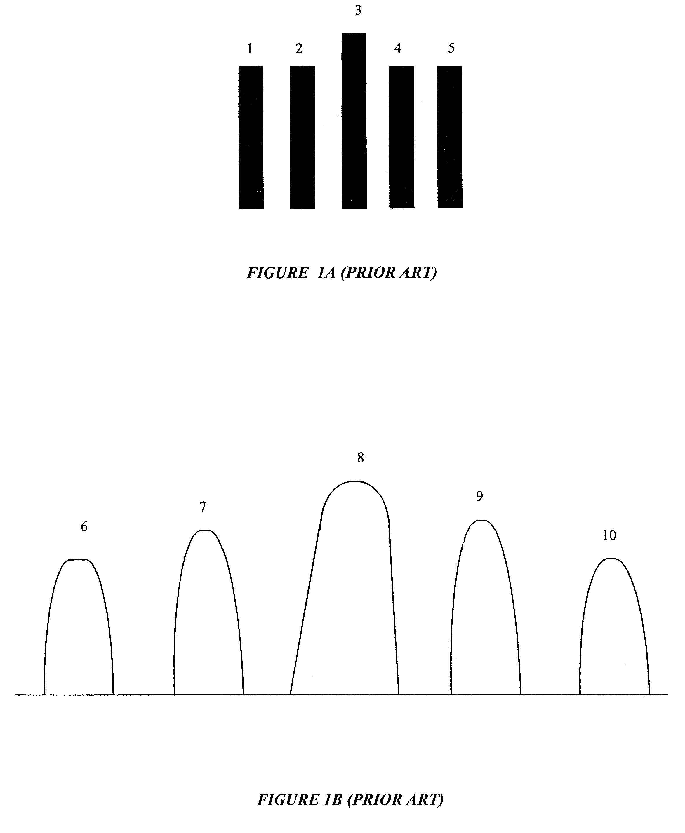
FIG. 1A is cross-sectional view of the prior art five-finger-bar test pattern. Traditional simple test pattern structures in masks like the five-finger-bar test pattern is used to measure the optical proximity effect on profile dimensions. The features or lines are classified according to the density or presence of neighboring lines, e.g., dense lines with many neighboring lines, isolated lines, and in-between lines with some neighboring lines. In FIG. 1A, the middle line 3 may classified as a dense line and the two lines on either side of the middle line, 1, 2, 4, and 5, would be in-between lines.

FIG. 1B is a cross-sectional view of the feature profile showing the optical proximity effect for the five-finger-bar test pattern. Features resulting from the five-finger-bar test pattern mask would have different profiles depending on the proximity and density of other features. For example, the center feature 8 has a bigger height and bottom width than the features at the edge of the te...


PUM

PropertyMeasurementUnit
widthaaaaaaaaaa
widthaaaaaaaaaa
optical metrology deviceaaaaaaaaaa

Abstract

The invention teaches a method and system for an accurate profile characterization of test patterns that may be implemented for real time use in a fabrication line. One embodiment is a non-destructive method for acquiring file data of the test pattern lines through the use of spectrum data measured with an optical metrology device and a profile library. The profile data comprise critical dimensions of all the test pattern lines included in the set of parameters to create the profile library. The test pattern lines may be designed to evaluate the effectiveness of measures to correct optical proximity, micro-loading or other process effects.

Description

BACKGROUND INVENTION1. Field of InventionInvention relates to the field of process metrology in semiconductor manufacturing and more particularly to the pattern process characterization in advanced lithography and etch technology.2. Description of Related ArtThe semiconductor industry is faced with the increased need to make features with smaller critical dimensions. To address this need, lithography processes had to be extended with techniques such as optical proximity correction, phase shifting, scattering bars, and off-axis illumination, allowing the industry to extend the life of deep ultraviolet lithography beyond the sub-wavelength barrier.In advanced lithography, the effect of optical proximity is pronounced and very significant. Optical proximity effect manifests itself in the features where the line ends become short or long depending on whether it is positive or negative resist is used, line widths increase or decrease based on local density patterns, corners are rounded i...

Claims


Application Information

Patent Timeline
Patent Type & Authority Patents(United States)
IPC IPC(8): G01N21/47G01N21/956G01N21/88G03F7/20G01N21/95G01N21/27G03F1/08H01L21/027H01L21/66
CPCG01N21/4788G03F7/70483G01N21/956G01N21/9501
Inventor NIU, XINHUIJAKATDAR, NICKHIL
Owner TIMBRE TECH INC
Why Eureka
Try Eureka