Externally excited torroidal plasma source with a gas distribution plate

a plasma source and gas distribution plate technology, applied in the field of plasma reactors, can solve the problems of slow and therefore relatively less productive, difficult to process plasma of such devices, and increase the processing difficulty of such devices, so as to increase the selectivity of etching to photoresist or other materials, and increase the plasma ion density

US6551446B1Inactive Publication Date: 2003-04-22APPLIED MATERIALS INC
37 Cites 95 Cited by

Patent Information

Authority / Receiving Office
US · United States
Patent Type
Patents(United States)
Current Assignee / Owner
Publication Date
2003-04-22
Estimated Expiration
Not applicable · inactive patent

Smart Images

  • Figure 1
    Figure 1
  • Figure 2
    Figure 2
  • Figure 3
    Figure 3
Patent Text Reader

Abstract

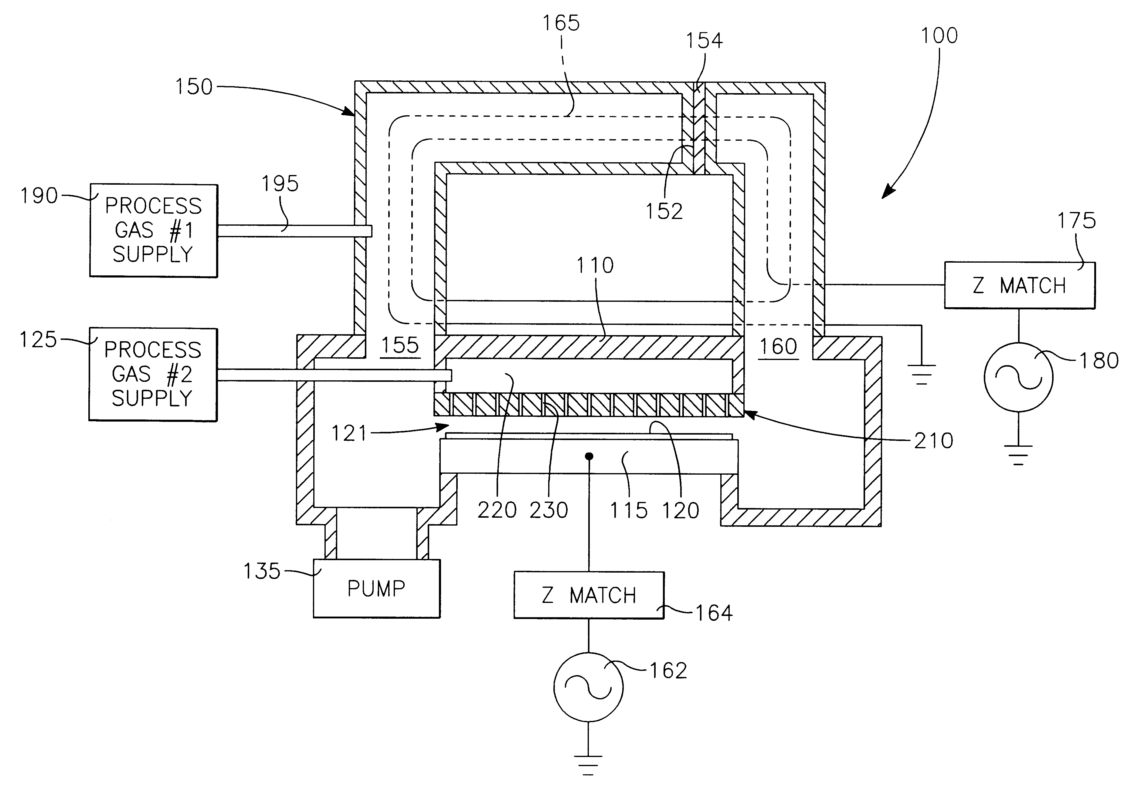
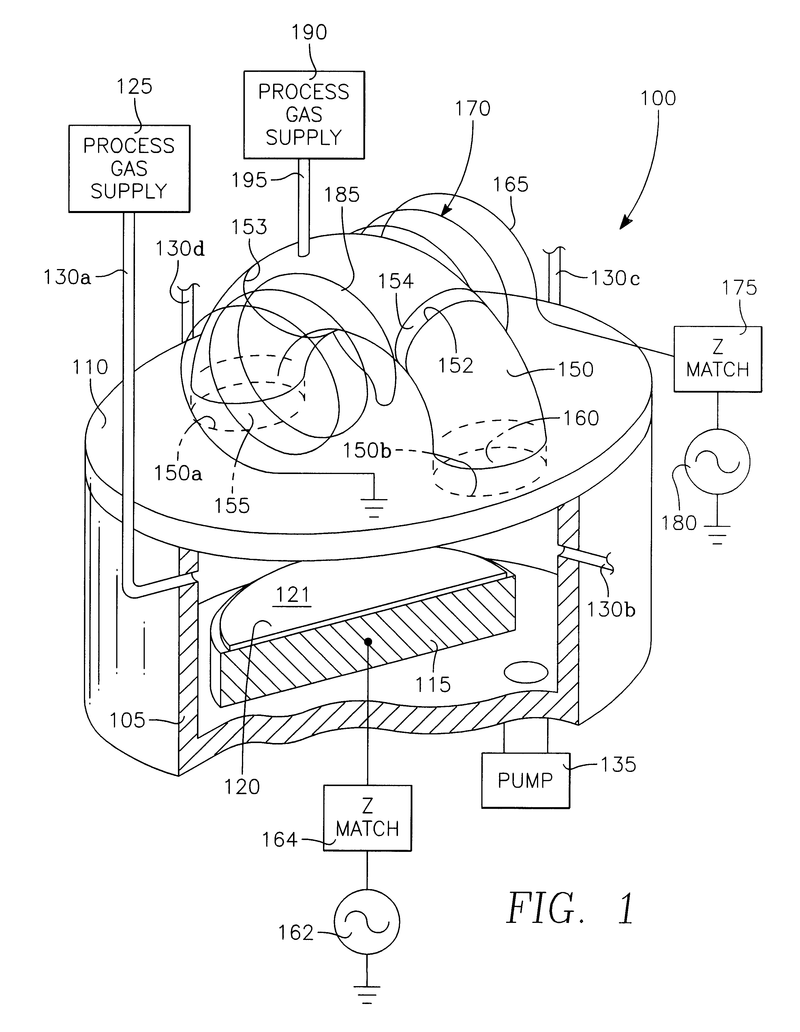
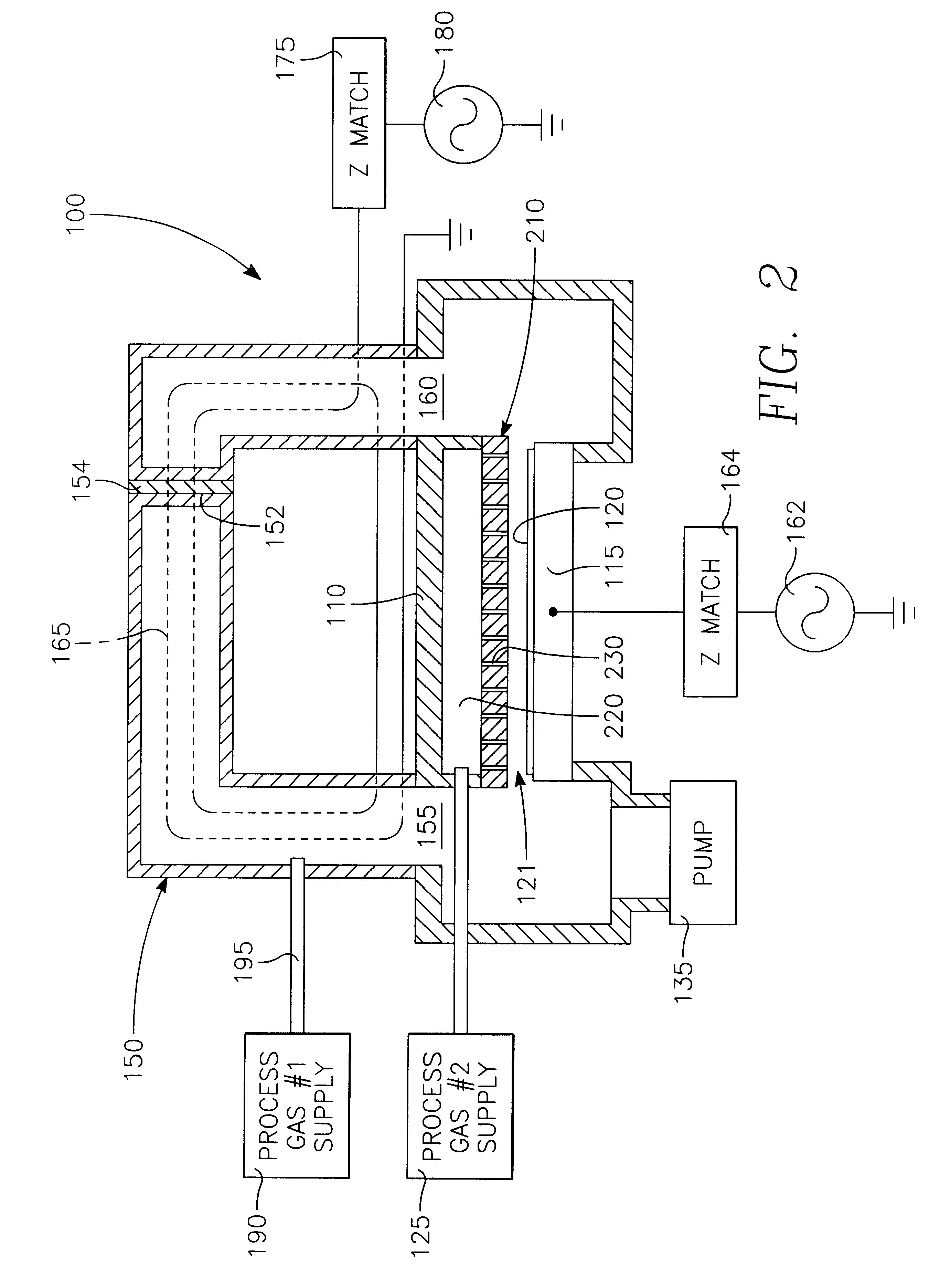
A plasma reactor for processing a workpiece includes a vacuum enclosure, including a wall, defining a vacuum chamber, the vacuum chamber having a main chamber portion on one side of the wall and a plenum on another side of the wall, the plenum communicating with the chamber portion through at least one opening in the wall, a workpiece support within the main chamber portion and facing the wall. A gas distribution plate is adjacent the wall and faces the workpiece support and is coupled to a reactive process gas supply for injecting reactive process gases directly into a process region adjacent the workpiece support. A gas injection port at the plenum is coupled to a diluent gas supply for injecting diluent gases into the plenum. A coil antenna adapted to accept RF power is inductively coupled to the interior of said plenum, and is capable of maintaining a plasma in a reentrant path through the plenum and across the process region.
Need to check novelty before this filing date? Find Prior Art

Description

1. Technical FieldThe invention concerns plasma reactors used in processing workpieces in the manufacturing of items such as microelectronic circuits, flat panel displays and the like, and in particular plasma sources therefor.2. Background ArtThe trend in microelectronic circuits toward ever increasing densities and smaller feature sizes continues to make plasma processing of such devices more difficult. For example, the diameter of contact holes has been reduced while the hole depth has increased. During plasma-enhanced etching of a dielectric film on a silicon wafer, for example, the etch selectivity of the dielectric material (e.g. silicon dioxide) to photoresist must be sufficient to allow the etch process to etch a contact hole whose diameter is ten to fifteen times its depth, without appreciably disturbing the photoresist mask defining the hole. This task is made even more difficult because the recent trend toward shorter wavelength light for finer photolithography requires a...

Examples

Embodiment Construction

:

FIG. 9 illustrates a modification of the embodiment of FIG. 1 in which the side antenna 170 is replaced by a smaller antenna 910 that fits inside the empty space between the ceiling 110 and the hollow conduit 150. Preferably, the antenna 910 is a single coil winding centered with respect to the hollow conduit 150.

FIGS. 10 and 11 illustrate how the embodiment of FIG. 1 may be enhanced by the addition of a closed magnetically permeable core 1015 that extends through the space between the ceiling 110 and the hollow conduit 150. The core 1015 improves the inductive coupling from the antenna 170 to the plasma inside the hollow conduit 150.

Impedance match may be achieved without the impedance match circuit 175 by using, instead, a secondary winding 1120 around the core 1015 connected across a tuning capacitor 1130. The capacitance of the tuning capacitor 1130 is selected to resonate the secondary winding 1120 at the frequency of the RF power source 180. For a fixed tuning capacitor 1130,...