Asynchronous latch design for field programmable gate arrays

a technology of asynchronous latches and gate arrays, applied in the field of logic devices, can solve problems such as the approach of essentially an open collector technique, the production of glitches in certain situations,

Inactive Publication Date: 2003-04-29
INT BUSINESS MASCH CORP
View PDF7 Cites 6 Cited by
  • Summary
  • Abstract
  • Description
  • Claims
  • Application Information

AI Technical Summary

Problems solved by technology

While this technique is very efficient, by its very nature can produce glitches in certain situations.
This approach is essentially an open collector technique and is hampered from a performance point of view since performance is limited by the inherently slow rise time (i.e., rc time constant) of the internal buses.

Method used


Image

  • Asynchronous latch design for field programmable gate arrays
  • Asynchronous latch design for field programmable gate arrays
  • Asynchronous latch design for field programmable gate arrays

Examples


Embodiment Construction

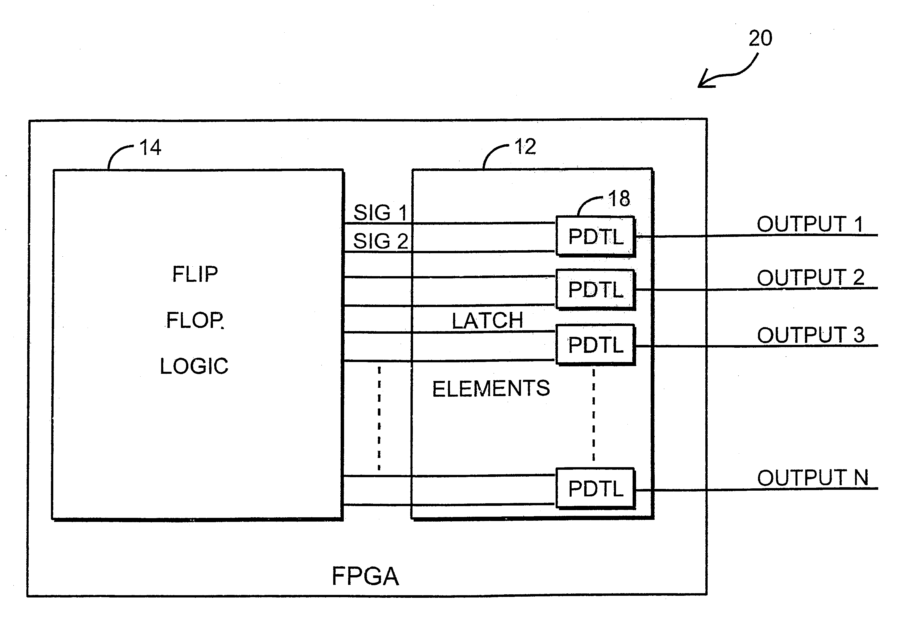
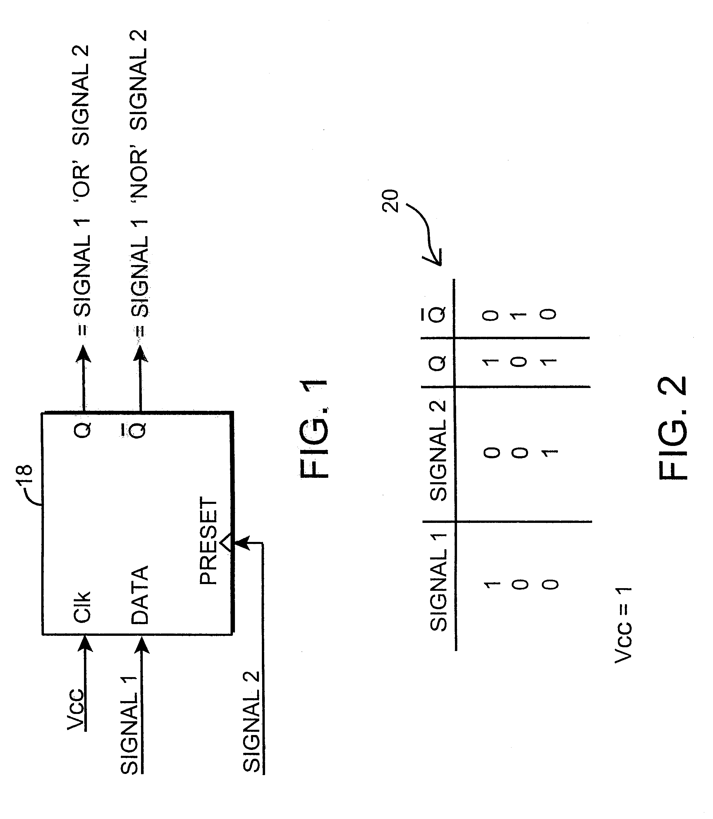
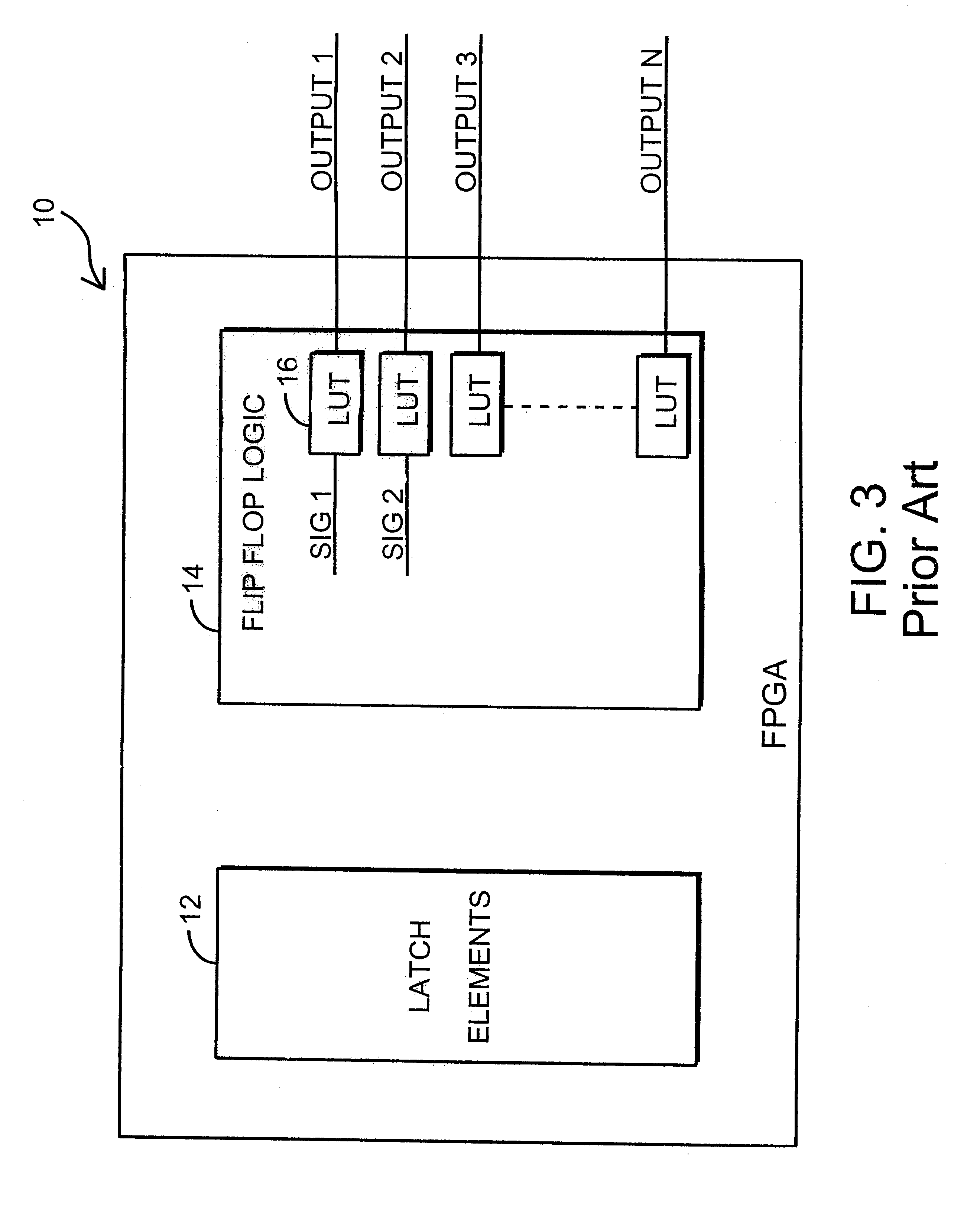
To solve the aforementioned glitch problems associated with asynchronous logic operations using LUTs in FPGAs, the present invention utilizes a preset dominant transparent latch element 18 to replace the LUT, as shown in FIG. 1. Since latch elements are normally present in FPGAs, as shown in FIG. 3, no additional circuitry is necessary to implement the approach of the present invention. Rather, the latch elements are programmed to preset dominant transparent latches, as described below. Essentially, the present invention utilizes a latch 18 already contained within the FPGA to implement the desired logic function normally associated with the look-up table.

In one exemplary embodiment shown in FIG. 1, the clock input of the latch 18 is held constant using the power supply signal VCC. Signal 1 is supplied to the data input and signal 2 is supplied to the preset input. Signal 1 and signal 2 represent flip-flop output signals, and are generally defined herein as intermediate output signa...


PUM


Abstract

A programmable logic circuit is provided that solves glitch problems associated with asynchronous logic operations associated with conventional look-up tables by utilizing a preset dominant transparent latch element to replace a conventional look-up table. Since latch elements are normally present in programmable logic circuits (e.g., FPGAs) no additional circuitry is necessary to implement the approach of the present invention. In one exemplary embodiment, an FPGA is provided which includes an array of programmable latch elements, and an array of programmable flip-flop elements generating flip-flop output signals. One or more of the latch elements are programmed to form a preset dominant transparent latch (PDTL) such that the data signals are coupled to the data inputs and preset inputs of the latch. In this manner, the latch operates to replace conventional look-up tables by operating as a primitive OR or NOR gate to generate a desired output.

Description

1. Field of the InventionThe present invention relates to logic device that uses a transparent latch technique to avoid glitches normally associated with RAM look-up tables. Particular utility of the present invention is found in field programmable gate arrays (FPGA), but has general applicability to any logic device.2. Description of Related ArtFIG. 3 depicts a conventional field programmable gate array (FPGA) 10. A typical FPGA comprises an array of programmable latch elements 12 and an array of programmable flip-flop logic elements 14. A plurality of flip flop elements are programmed to operate as RAM devices formed into a look up table (LUT) 16 to generate a specified output given two or more input logic signals. Each look-up table receives two or more input signals, designated as signal 1 and signal 2, and generates an output signal, for example, output 1, output 2, output 3, . . . output n. When designing with FPGAs, general logic is normally implemented using RAM look-up tabl...

Claims


Application Information

Patent Timeline
Patent Type & Authority Patents(United States)
IPC IPC(8): H03K19/177
CPCH03K19/1774H03K19/17728
Inventor GARCIA, ENRIQUE
Owner INT BUSINESS MASCH CORP
Why Eureka
Try Eureka