Active matrix organic EL display device and method of forming the same

a display device and organic technology, applied in the direction of luminescent screen, discharge tube, identification means, etc., can solve the problems of display defect or display contrast reduction, increase in leakage current of thin film transistor, and increase in the severity of the problem

Inactive Publication Date: 2003-07-22
GOLD CHARM LTD
View PDF8 Cites 159 Cited by
  • Summary
  • Abstract
  • Description
  • Claims
  • Application Information

AI Technical Summary

Problems solved by technology

The incidence of the stray lights into the polysilicon layer 12 causes the increase in leakage of current of the thin film transistor and the transistor shows a malfunction, whereby a display defect or a display contrast reduction may be caused.
This problem becomes more serious as the display gradation becomes large.
If the circuitry includes a capacitor and the stray light is incident into a capacitive dielectric layer of the capacitor, then the capacitor becomes unable to hold charges.
The luminescence is, however, omnidirectional.
The above conventional optical shielding structures are unable to shield the circuitry such as the thin film transistor from the stray light particularly transmitted in the horizontal direction.

Method used


Image

  • Active matrix organic EL display device and method of forming the same
  • Active matrix organic EL display device and method of forming the same
  • Active matrix organic EL display device and method of forming the same

Examples


first embodiment

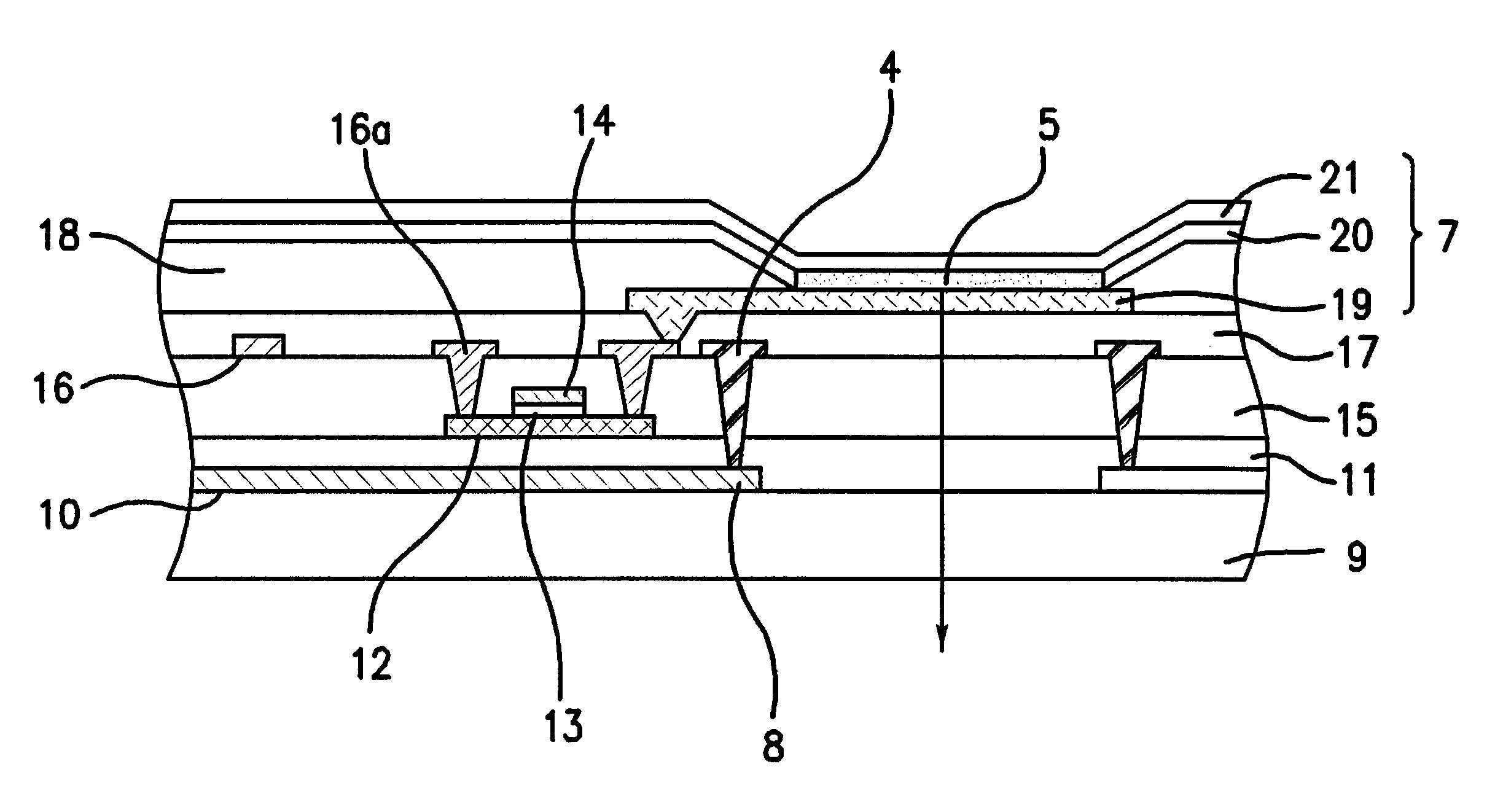
A first embodiment according to the present invention will be described in detail with reference to the drawings. FIG. 4 is a fragmentary plan view of a single pixel of an active matrix organic electroluminescence display device in a first embodiment in accordance with the present invention. FIG. 5 is a fragmentary enlarged plan view illustrative of a connecting portion between a thin film transistor and an indium tin oxide film in each pixel of FIG. 4. FIG. 6 is a fragmentary cross sectional elevation view illustrative of a single pixel of an active matrix organic electroluminescence display device, taken along a A-A' line of FIG. 4.

Each pixel is defined by row wirings 1 and column wirings 2. The pixel includes a circuit region and an organic EL device 7. The circuit region includes a thin film transistor 3 and a capacitor if any. A gate electrode 14 of the thin film transistor 3 is connected to the row wiring 1. One of source / drain terminals of the thin film transistor 3 is connec...

second embodiment

A second embodiment according to the present invention will be described in detail with reference to the drawings. FIG. 7 is a fragmentary enlarged plan view illustrative of a connecting portion between a thin film transistor and an indium tin oxide film in each pixel of an active matrix organic electroluminescence display device in a second embodiment in accordance with the present invention. FIG. 8 is a fragmentary cross sectional elevation view illustrative of a single pixel of an active matrix organic electroluminescence display device, taken along a B-B' line of FIG. 7.

Each pixel is defined by row wirings 1 and column wirings 2. The pixel includes a circuit region and an organic EL device 7. The circuit region includes a thin film transistor 3 and a capacitor if any. A gate electrode 14 of the thin film transistor 3 is connected to the row wiring 1. One of source / drain terminals of the thin film transistor 3 is connected to the column wiring 2. Another of the source / drain termi...

third embodiment

A third embodiment according to the present invention will be described in detail with reference to the drawings. FIG. 9 is a fragmentary enlarged plan view illustrative to a connecting portion between a thin film transistor and an indium tin oxide film in each pixel of an active matrix organic electroluminescence display device in a third embodiment in accordance with the present invention. FIG. 10 is a fragmentary cross sectional elevation view illustrative of a single pixel of an active matrix organic electroluminescence display device, taken along a C-C' line of FIG. 9.

Each pixel is defined by row wirings 1 and column wirings 2. The pixel includes a circuit region and an organic EL device 7. The circuit region includes a thin film transistor 3 and a capacitor if any. A gate electrode 14 of the thin film transistor 3 is connected to the row wiring 1. One of source / drain terminals of the thin film transistor 3 is connected to the column wiring 2. Another of the source / drain termin...


PUM


Abstract

The present invention provides an active matrix organic electroluminescence display device including: a transparent substrate; a plurality of pixels aligned over the transparent substrate, wherein each of the pixels further includes: a luminescent region which exhibits a luminescence upon application of an electric field; a circuitry region including at least a circuitry; and an optical shielding structure provided between the luminescent region and the circuitry region for shielding the circuitry region from the luminescence from the luminescent region.

Description

1. Field of the InventionThe present invention relates to an active matrix organic electroluminescence display device and a method of forming the same, and more particularly to an improvement in a pixel structure of the active matrix organic electroluminescence display device and a method of forming the pixel structure.2. Description of the Related ArtThe active matrix organic electroluminescence display device has an array of pixels, each of which includes a circuitry region and an electroluminescence region which exhibits a luminescence upon application of an electric filed. The circuitry region may often include a thin film transistor having a polysilicon layer.One of the conventional active matrix organic electroluminescence display device is disclosed in Japanese laid-open patent publication No. 2000-172198. FIG. 1A is a fragmentary plan view illustrative of a single pixel structure of the conventional active matrix organic electroluminescence display device. FIG. 1B is a fragm...

Claims


Application Information

Patent Timeline
Patent Type & Authority Patents(United States)
IPC IPC(8): H01L27/28H01L27/32H01L51/50H01L51/52G09F9/30H01L29/786H05B33/00H05B33/10H05B33/14H05B33/22H05B33/26
CPCH01L27/3272H01L29/78633H01L51/5281H10K59/126H10K59/8791H05B33/00H10K50/86
Inventor IMURA, HIRONORI
Owner GOLD CHARM LTD
Why Eureka
Try Eureka