Unlock instant, AI-driven research and patent intelligence for your innovation.

Liquid crystal panel, display device, identification mark detection device, detection display system, TFT array repair device and identification mark detection method

a display device and identification mark technology, applied in the field of display devices, can solve the problems of not always being able to specify the position finely and accurately, and it is difficult to finally identify which transistor actually is malfunctioning, and achieve the effect of processing the pixel regions of the display device effectively

Inactive Publication Date: 2003-07-22
AU OPTRONICS CORP
View PDF11 Cites 79 Cited by
  • Summary
  • Abstract
  • Description
  • Claims
  • Application Information

AI Technical Summary

Benefits of technology

is to provide an apparatus and a method, which are capable of a processing concerning pixel regions of the display device effectively.

Problems solved by technology

However, although the logic address of the malfunctioning transistor is known, it has been extremely difficult to finally identify which transistor actually is malfunctioning.
When the transistor exhibits micro defects within it, the decision has been impossible only by the video.
Accordingly, it was not always possible to specify the position finely and accurately.

Method used


Image

  • Liquid crystal panel, display device, identification mark detection device, detection display system, TFT array repair device and identification mark detection method
  • Liquid crystal panel, display device, identification mark detection device, detection display system, TFT array repair device and identification mark detection method
  • Liquid crystal panel, display device, identification mark detection device, detection display system, TFT array repair device and identification mark detection method

Examples


Embodiment Construction

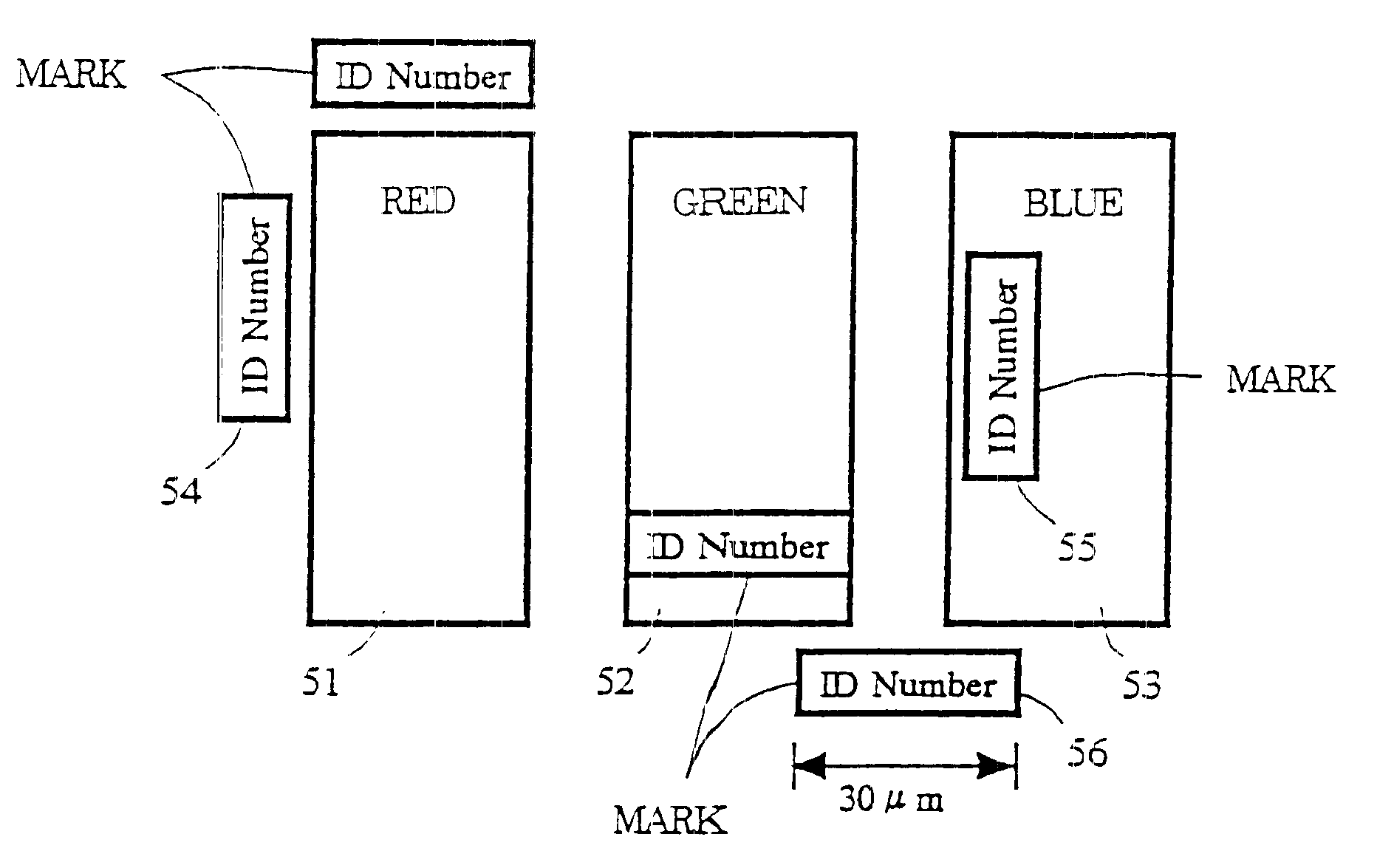
Descriptions for an embodiment in which an identification mark is formed in a pixel region of a TFT (Thin-Film Transistor) array in a TFT liquid crystal module and the identification mark is detected will be made. Furthermore, as an example using this identification mark, a repair device for specifying a repair position of the TFT array in a repair process and an information processing device which accepts a screen input using a laser pen will be described.

TFT (Thin-Film Transistor) Liquid Crystal Module

A structure of the TFT liquid crystal module to which the identification mark is formed will be described. FIG. 1 is a figure showing a schematic constitution of a color TFT (Thin-Film Transistor) liquid crystal module according to an embodiment of the present invention. In FIG. 1, reference numeral 11 denotes a color TFT liquid crystal module; 12, a TFT liquid crystal panel having a plurality of pixel regions; 13, a driving circuit comprising a LSI for driving electrically the TFT l...


PUM


Abstract

In each pixel region 41 of a liquid crystal TFT array substrate, formed are an ITO transparent electrode 43, a gate line 48, a data line 46, a TFT active device 45, an identification mark 50 and the like. The identification mark 50 is provided by forming a bar code made of silver on the gate line 48. Since the identification mark 50 is formed within the pixel region 41, a transistor to be repaired can be surely identified, for example, by detecting the identification mark in a repair processing of the TFT array substrate. Furthermore, in an information processing apparatus for inputting figures and characters onto a screen using a laser pen, a locus of the laser pen can be accurately specified by specifying a position of a pixel region from an identification mark detected by the laser pen, and the figures and the characters input can be recognized minutely.

Description

1. Technical FieldThe present invention relates to a display device, more particularly relates to a display device having an identification mark in its pixel region.2. Prior ArtAs a first prior art, a repair processing for a TFT array of a liquid crystal display panel will be described. When at least one of transistors as an active device on a TFT array is malfunctioning in manufacturing the liquid crystal display panel, conventionally the transistor is fused by a laser beam, and a repair processing is carried out to keep the malfunctioning transistor at a short-circuited state. In this repair processing, an electrical measurement is carried out as a pre-step, and a logic address of the malfunctioning transistor iscidentified. This electrical measurement is performed in such manner that all transistors on the TFT array are driven, and if any of them is malfunctioning, the malfunctioning transistor is detected and its logic address is output.In a repair apparatus the TFT array is fix...

Claims


Application Information

Patent Timeline
IPC IPC(8): G02F1/133G02F1/13G02F1/1362G06F3/033G06F3/041G02F1/136G02F1/1368G06F3/03
CPCG02F1/13338G02F1/136259G06F3/0317G06F3/03545G06F3/0321
Inventor KATSU, YOSHIHIROYAMASHITA, HIROSHIKIMURA, YASUHIROTSUJI, SATOSHI
Owner AU OPTRONICS CORP