Method and system for controlling the photolithography process

a photolithography and process technology, applied in the field of photolithography process control methods and systems, can solve the problems of incompatibility of values and high cost of cd tool 7 devices, and achieve the effect of improving the accuracy of results

Inactive Publication Date: 2003-11-04
NOVA MEASURING INSTR LTD
View PDF2 Cites 23 Cited by
  • Summary
  • Abstract
  • Description
  • Claims
  • Application Information

AI Technical Summary

Problems solved by technology

The CD tool 7 is an expensive "stand alone" device which is typically manually loaded / unloaded.
However, the wafer W under processing has certain real values of the above parameters, which values may not match the expected ones, owing to the incoming substrate, PR materials and coating tools variations.

Method used


Image

  • Method and system for controlling the photolithography process
  • Method and system for controlling the photolithography process
  • Method and system for controlling the photolithography process

Examples


example

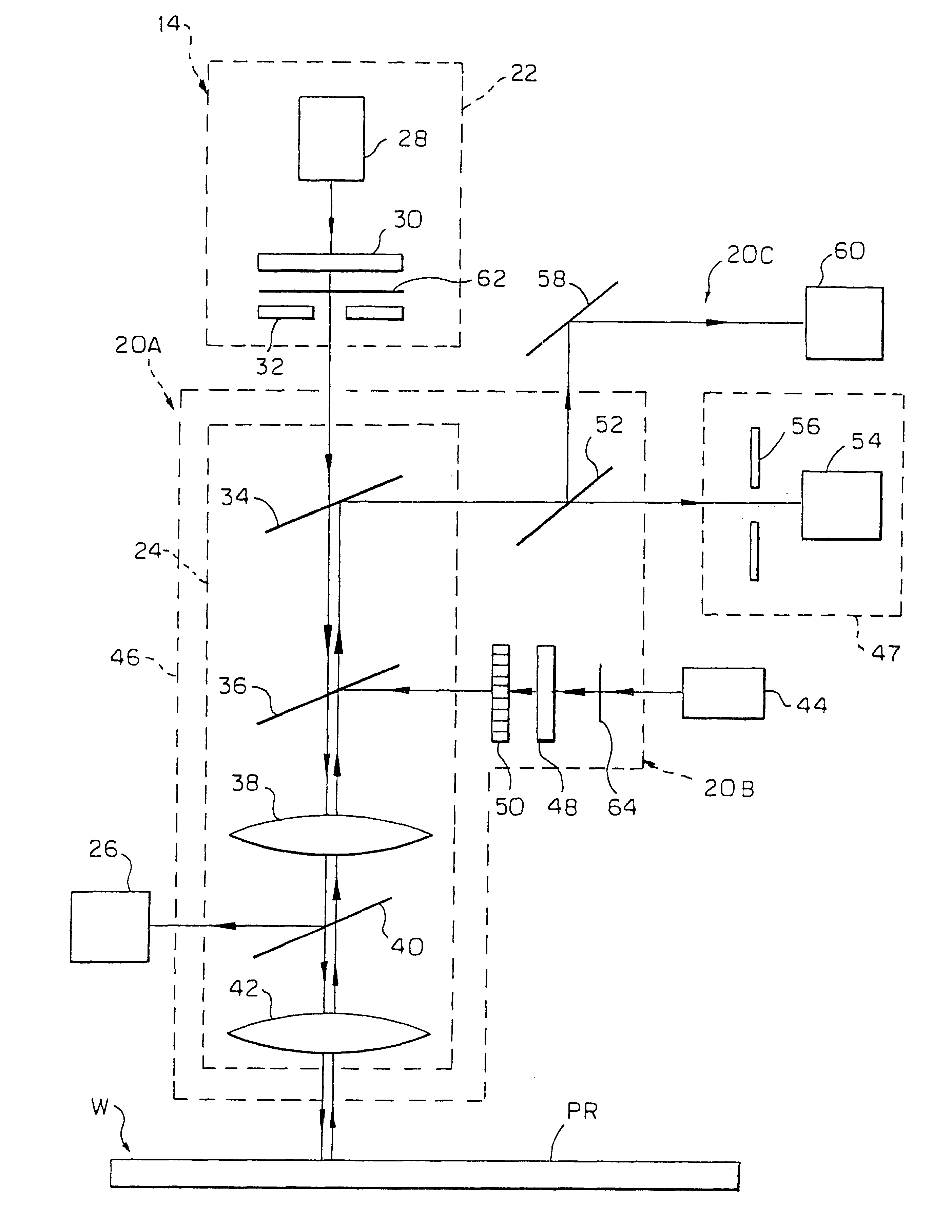
In this example, .delta.R=0, .DELTA.h=0. Turning back to FIGS. 4a and 4b, the calibration curves are obtained. In other words, the relevant data base is already created as described above. The recommended exposure dose is as follows:

d.sub.rec =4 mJ / cm.sup.2

The calibration curves C.sub.1 and G.sub.1 show that for this dose value we have:

k.sub.c =0.006417; (.differential.d / .differential.k).sub.c =-375.37

Considering the typical case that a dose correction is needed, the second operational stage is performed, i.e. the exposure with the recommended exposure dose is applied to the measurement site, and the measured (calculated) data for the absorption coefficient is determined to be:

k.sub.m =0.005636

As seen in the calibration curves C.sub.1 and G.sub.1 for the measured value k.sub.m of the absorption coefficient, we have:

d.sub.m.apprxeq.4.5 mJ / cm.sup.2 (.differential.d / .differential.k).sub.m =-393.3

Using the above equation for the corrected dose value, we have: ##EQU3##

Hence, in order to ...


PUM

PropertyMeasurementUnit
processing timeaaaaaaaaaa
optical modelaaaaaaaaaa
critical dimensionsaaaaaaaaaa

Abstract

A method and measuring tool are presented for automatic control of photoresist-based processing of a workpiece progressing through a processing tool arrangement. Spectrophotometric measurements are applied to the workpiece prior to being processed, spectral characteristics of the workpiece are measured, thereby obtaining measured data indicative of at least one parameter of the workpiece that defines an optimal value of at least processing time parameter of the processing tool to be used in the processing of said workpiece to obtain certain process results. This data is analyzed to determine data indicative of the optimal value of said at least processing time parameter, and thereby enable calculation of a correction value to be applied to said processing time parameter prior to applying the processing tool to the workpiece.

Description

The present invention is in the field of measuring / inspecting techniques and relates to a method and a system for controlling the operation of a processing tool for processing workpieces. The invention is particularly useful in the manufacturing of semiconductor devices to control the operation of photolithography tools to optimize the entire photolithography process.The manufacture of semiconductor devices consists of several procedures applied to a semiconductor wafer to define active and passive elements. The wafer is prepared and one or more layers are deposited thereon. Thereafter, the process of photolithography is performed, in which the surface of a wafer with a pattern conforming to circuit elements is formed. An etching process applied to the uppermost layer follows the photolithography. By desirably repeating these processes, a multi-level semiconductor wafer is produced. Thus, photolithography is one of the main steps in the manufacture of semiconductor devices. It actua...

Claims


Application Information

Patent Timeline
Patent Type & Authority Patents(United States)
IPC IPC(8): G03F7/20H01L21/027B82B1/00
CPCG03F7/70558
Inventor COHEN, YOELFINAROV, MOSHE
Owner NOVA MEASURING INSTR LTD
Why Eureka
Try Eureka