Method for producing contactless chip cards and corresponding contactless chip card

a technology of contactless chip and chip card, which is applied in the direction of sensing record carriers used with machines, instruments, etc., can solve the problems of high production cost of coil and chip card, difficult connection between the thick wires of the coil and the naked chip, and disadvantageous thermal and mechanical stability

Inactive Publication Date: 2003-11-25
PAC TECH PACKAGING TECH
View PDF24 Cites 47 Cited by
  • Summary
  • Abstract
  • Description
  • Claims
  • Application Information

AI Technical Summary

Benefits of technology

Bumps also have the advantage that they can be used for adjusting a minimum distance to the (base) surface in the recesses, whereby the risk of destroying the chip when the chip is being aligned and contacted is substantially reduced. In addition, it is then not necessary that this distance control is carried out by the contacting means.
The present invention permits on the basis of very few method steps the production of a card body which includes at least one recess, especially by injection moulding the card body by means of thermoplastic materials, and which has a structured metallization applied to the card surface including the recess. This allows a simple and economy-priced production of cards in high numbers of pieces. In addition, the chip cards produced according to the present invention are characterized by a high mechanical stability and reliability. This is due to the small number of layers of which the chip card consists and it is due to the fact that the conductor tracks are directly applied to the one-piece card body according to a conductor track pattern, especially a coil. Hence, problems caused by incompatible materials will not arise in the case of the chip card according to the present invention. Furthermore, it is not necessary to use an intermediate carrier for the coil in this kind of chip card. Another advantage is the possibility of using the flip-chip technique for contacting the chip, which means that the advantages of a simple sequence of process steps and of a small overall height can be utilized. Moreover, a wire-bondable metallization is not necessary in this case. A further advantage is that the expensive and sensitive chips are incorported in the card body only in a very late method step and are therefore exposed to detrimental thermal, chemical and physical loads to a much lesser degree by the few method steps which may perhaps be carried out afterwards. In particular, the chips are not exposed to the thermal load of an injection-moulding process according to the present invention. This guarantees, in the. final analysis, a lower reject rate and a higher reliability as well as a longer service life of the cards produced.

Problems solved by technology

Disadvantages of this method are primarily the difficult application of the coil to the chip card and the connections between the thick wires of the coil and the naked chip.
Disadvantages of this method are the high production costs of the coil and the difficulties which have to be overcome when the whole card body is laminated.
The lamination is, moreover, disadvantageous with regard to the thermal and the mechanical stability and, consequently, with regard to the service life of the chip card.
In particular, the temperatures prevailing when the carrier is enclosed with the chip card material by injection moulding have a negative effect on the function of the expensive semiconductor chips.
Furthermore, mistakes in the injection moulding process, i.e. mistakes in a comparatively economy-priced plastic component, will have the effect that the card including the expensive semiconductor chip becomes a reject.
This method requires, however, an additional stamping process for the chip reception area and a complicated laminating and coating process.

Method used


Image

  • Method for producing contactless chip cards and corresponding contactless chip card
  • Method for producing contactless chip cards and corresponding contactless chip card
  • Method for producing contactless chip cards and corresponding contactless chip card

Examples


Embodiment Construction

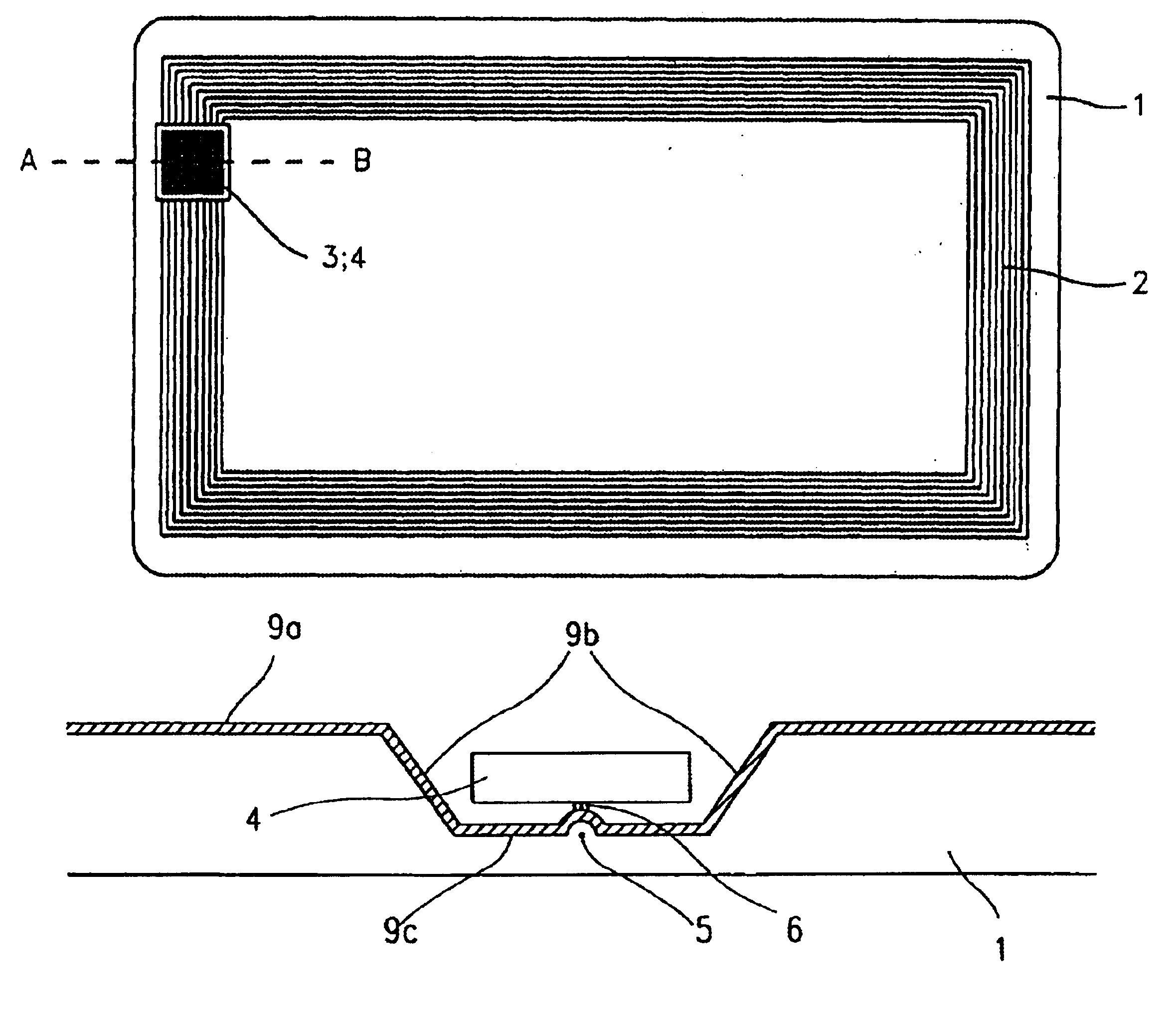
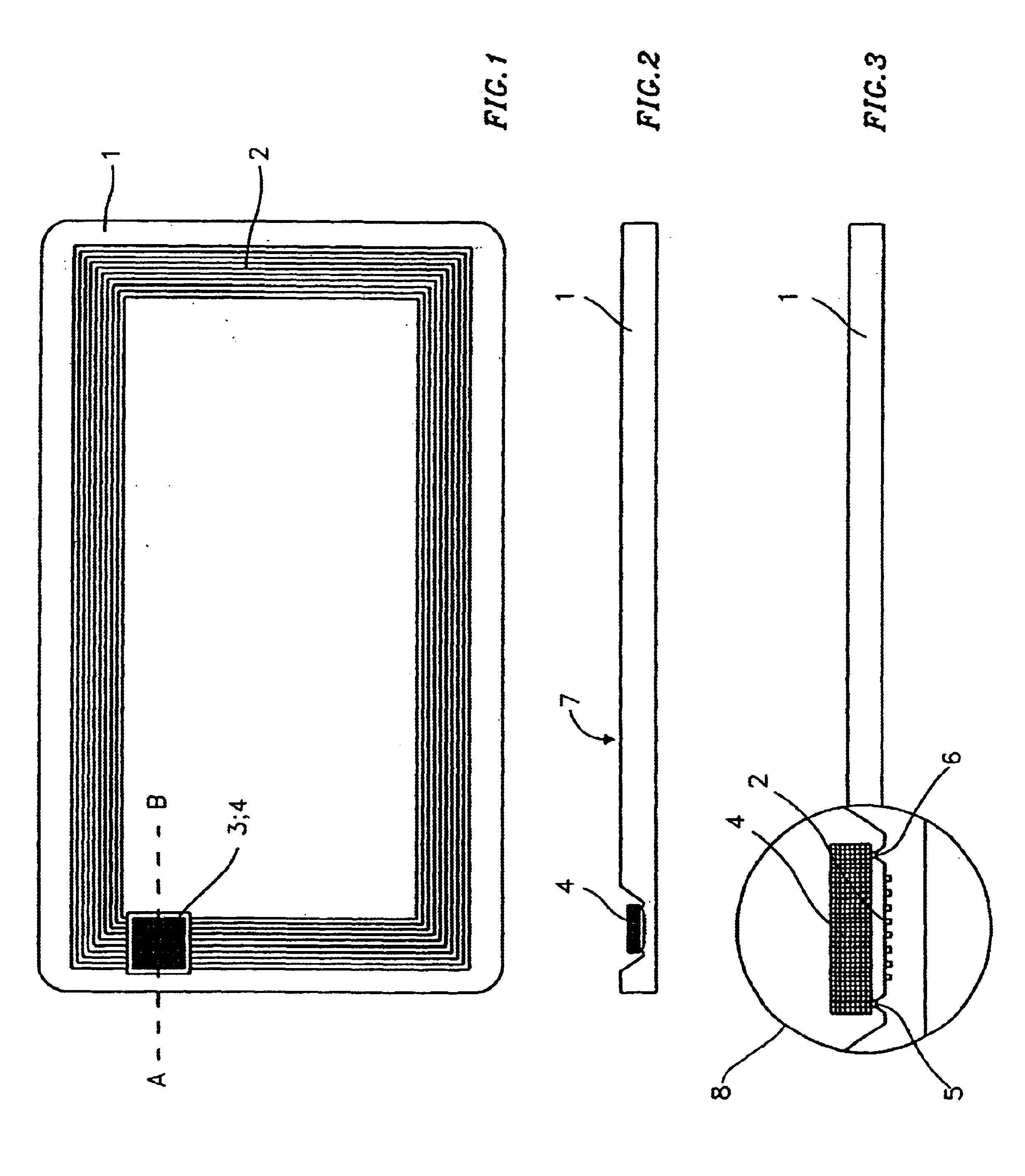
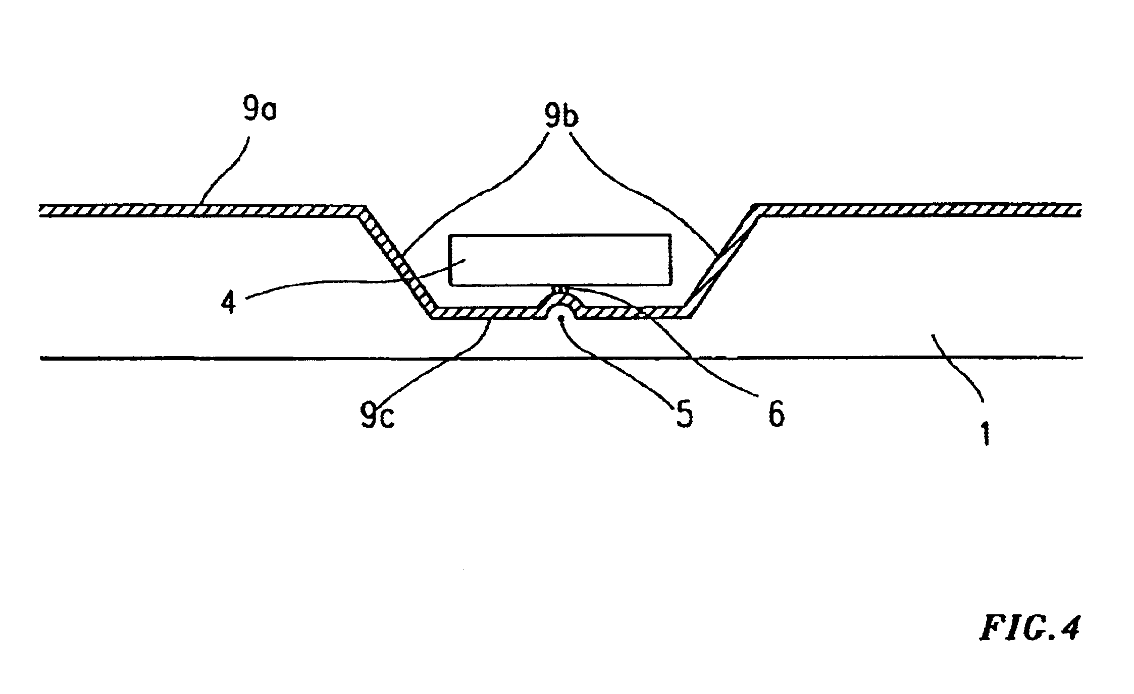
In one embodiment, the chip card 1 includes precisely a single recess 3 in which a square chip 4 is aligned and contacted with the conductor tracks of the coil 2. The shape and the size of the recess has been adapted to the shape of the chip. From FIG. 2 it can be seen that the depth of the recess has been chosen such that the contacted chip is fully submerged in the recess, i.e. it does especially not project above the card surface 7. FIG. 3 shows an enlarged sectional view 8 of the recess area of the chip card, the plane of section being orthogonal to the conductor tracks (conductor tracks extending in the direction of the normal vector of the sectional area). The bumps 5 formed from the card body material 1, the material 6 used for actual contacting, an adhesive or a solder, and the conductor tracks of the coil 2 are clearly visible in this cross-sectional view. FIG. 4 shows a cross-sectional view through the recess with an impressed coil, the plane of section being orthogonal to...


PUM


Abstract

The present invention relates to a method of producing a contactless chip card. In a first step of the method, a card body with one or a plurality of recesses on one card body side is produced from a theremoplastic material, preferably by injection moulding. Bumps being formed on the base surface of the recesses. Subsequently, conductor tracks corresponding to a coil as a conductor track pattern are impressed directly onto surface areas of the card body side including the recesses using a hot impressing technique. The conductor tracks are impressed especially also onto surface areas inside the recesses such that same extends across the bumps. One or a plurality of chips are then aligned in the recesses and contacted with the conductor tracks in the recesses which extend across the bumps. The method according to the present invention is advantageous insofar as it permits a simple production of a chip card, which requires only a few method steps and is therefore also economical. Furthermore, such a chip card is both mechanically stable and reliable, since it comprises very few individual layers and since the conductor tracks of the coil are applied directly to the card body.

Description

1. Field of the InventionThe present invention relates to a method of producing contactless chip cards including at least one chip and to a contactless chip card.A great number of chip cards is nowadays already used in all fields of private and public life. Their efficiency can be increased still further by using modern integrated circuits, since by implementing application-specific functions in the chip the field of application of chip cards can be extended to the following fields exceeding the sphere of identification and telecommunications: in the public health service e.g. by the insured person's card, the patient's data card and the emergency card. In the field of communication, chip cards can be used for controlling access to communication networks and for service payments as well as for data encryption and data protection. In payment transcations chip cards are very suitable to be used as cheque cards, credit / debit cards, electronic purses and for charge accounting for local ...

Claims


Application Information

Patent Timeline
Patent Type & Authority Patents(United States)
IPC IPC(8): G06K19/077G06K19/07
CPCG06K19/07749G06K19/0775G06K19/07783G06K19/07779H01L2224/16225H01L2224/16227
Inventor ZAKEL, ELKEASCHENBRENNER, ROLFANSORGE, FRANKKASULKE, PAUL
Owner PAC TECH PACKAGING TECH
Why Eureka
Try Eureka