Flip chip substrate design

a chip substrate and flip chip technology, applied in the field of flip chip substrate design, can solve the problems of limiting the ability to form thin packages, inefficient manufacturing processes of these devices, and many bga (ball grid array) substrates that do not have the capability for pre-attaching or forming cavities

Inactive Publication Date: 2003-12-09
SEMICON COMPONENTS IND LLC
View PDF2 Cites 74 Cited by
  • Summary
  • Abstract
  • Description
  • Claims
  • Application Information

AI Technical Summary

Problems solved by technology

Additionally, many BGA (ball grid array) substrates do not have the capability for solder balls to be pre-attached or for a cavity to be milled in the substrate to

Method used


Image

  • Flip chip substrate design
  • Flip chip substrate design
  • Flip chip substrate design

Examples


Embodiment Construction

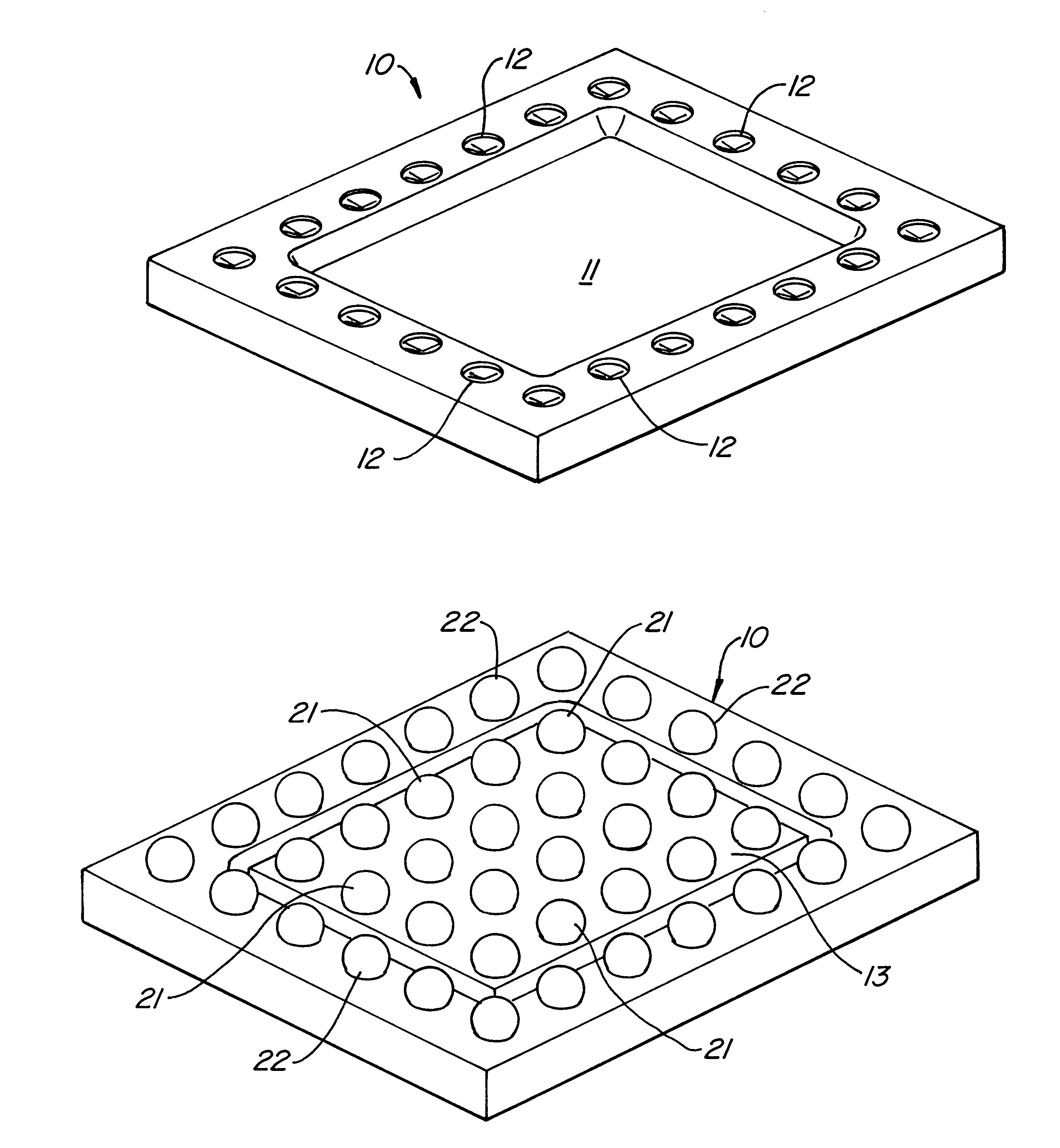
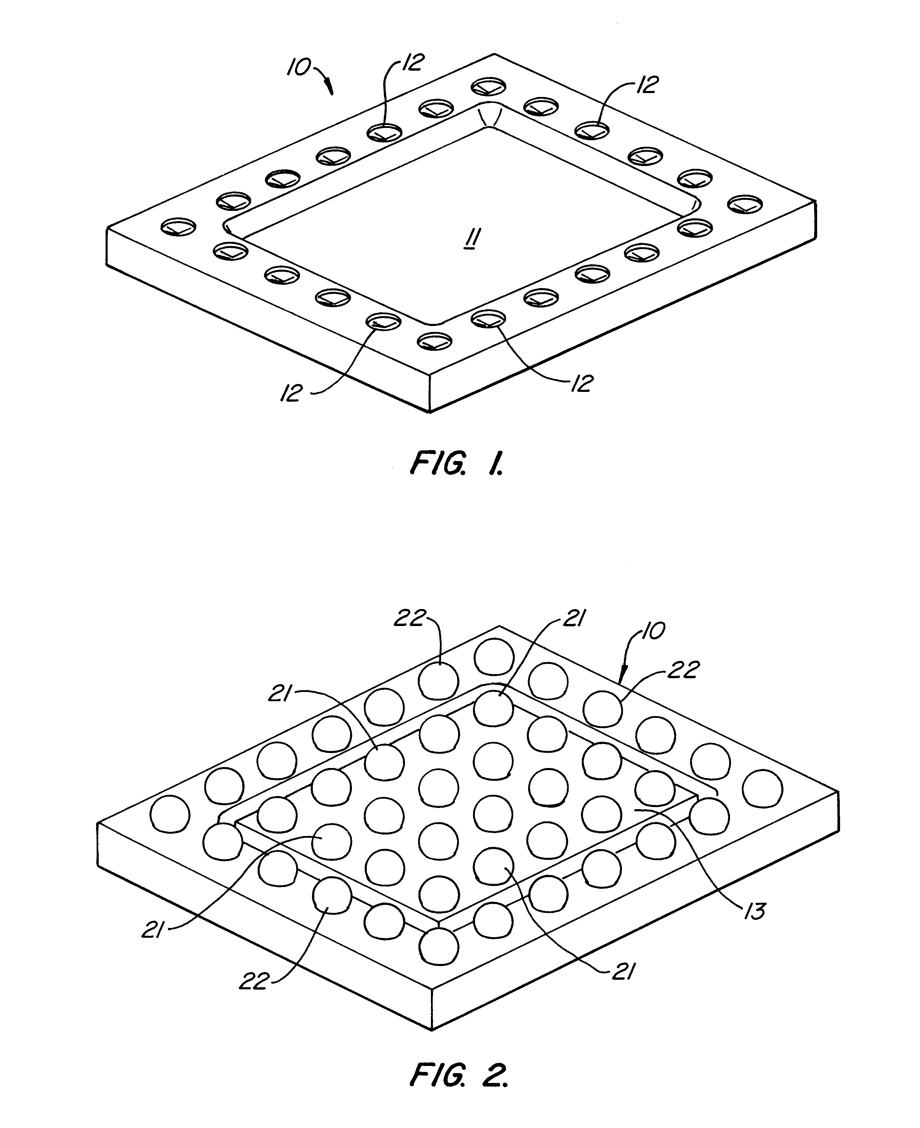
FIG. 1 illustrates a leadframe 10 for use in manufacturing a chip device in accordance with the present invention. The leadframe includes a die attach cavity 11 defined within the leadframe. In a preferred embodiment, a plurality of dimples 12 are defined around the periphery of the leadframe.

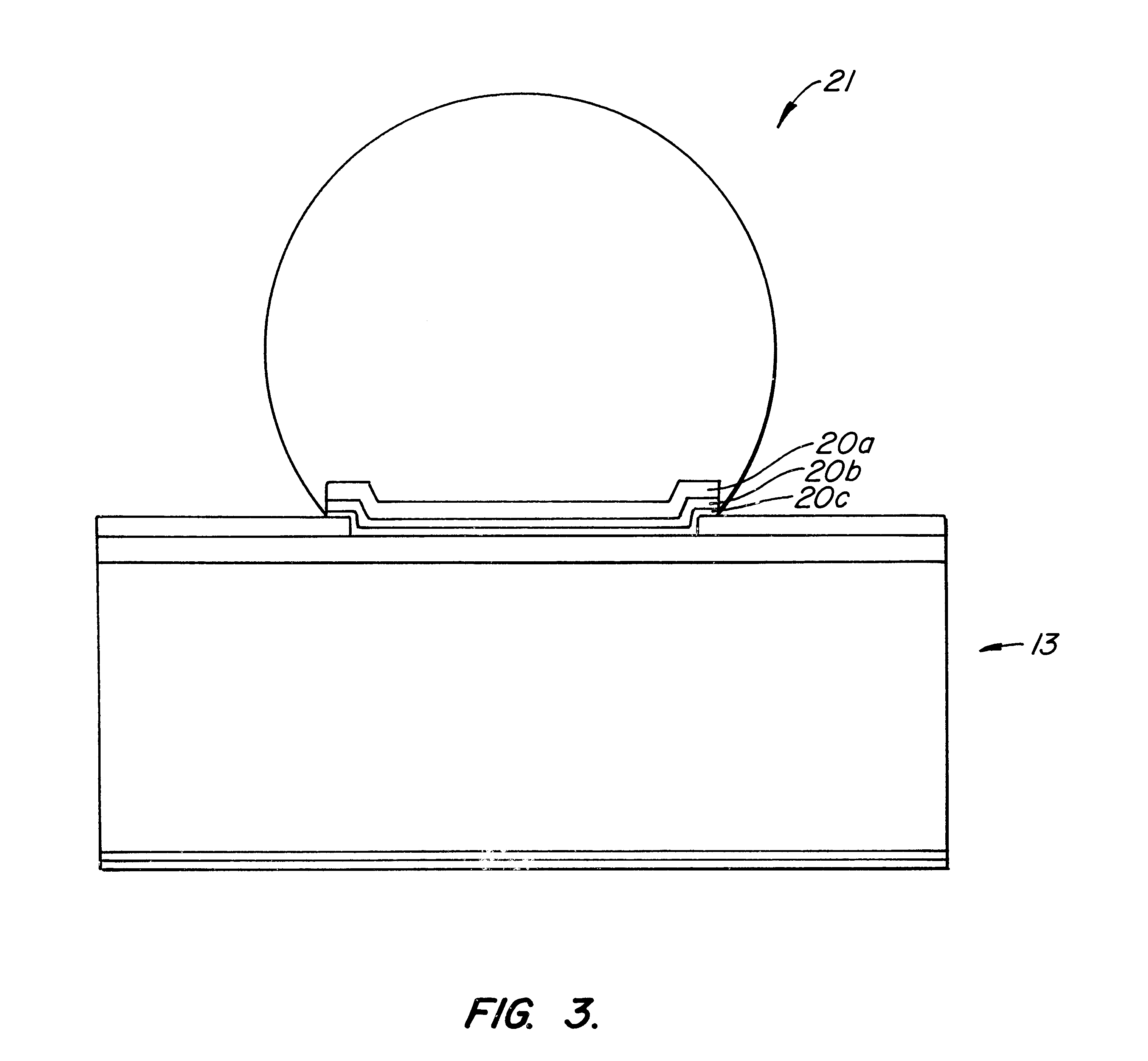
As can be seen in FIG. 2, a die 13 is placed within the cavity to complete the chip device. Die 13 is preferably a one-piece item that is often referred to in the art as a "bumped die." As can be seen in FIG. 3, a bumped die includes die 13, "under bump material" that serves as an intermediate layer 20 between the top surface of the die and solder bump 21, and the solder bumps themselves. Preferably, the under bump material is one of TiW, Cu, Au or an equivalent. In the example illustrated in FIG. 3, the under bump material is broken into three layers--Cu plating 20a, sputtered Cu 20b and sputtered Ti 20d.

The die attach pad area is etched out such that the depth of the cavity is the same as the...


PUM

PropertyMeasurementUnit
Thicknessaaaaaaaaaa
Electrical resistanceaaaaaaaaaa
Thermal resistanceaaaaaaaaaa

Abstract

A chip device that includes a leadframe that has a die attach cavity. The memory device further includes a die that is placed within the die attach cavity. The die attach cavity is substantially the same thickness as the die. The die is positioned within the cavity and is attached therein with a standard die attachment procedure.

Description

1. Field of the InventionThe present invention relates to a chip device, and more particularly, to discrete power components such as MOSFETs, as well as ICs such as memory circuits that include a leadframe that includes a cavity for receiving the die.2. Description of the Prior ArtChip devices generally include a leadframe and a bumped die attached thereto. Many of the packages are multiple pieces and rely on wire bonding as the interconnect between the die and the package. Additionally, many BGA (ball grid array) substrates do not have the capability for solder balls to be pre-attached or for a cavity to be milled in the substrate to facilitate die attach.These prior art packages limit the ability to form thin packages. Additionally, the manufacturing processes for these devices are inefficient.The present invention provides a chip device that includes a die and a leadframe. The leadframe includes a die attach cavity. The die attach cavity is substantially the same thickness as the...

Claims


Application Information

Patent Timeline
IPC IPC(8): H01L23/04H01L23/02H01L23/28H01L23/31H01L23/12
CPCH01L23/041H01L24/05H01L23/3107H01L2224/0554H01L24/13H01L24/14H01L24/16H01L2224/0401H01L2224/131H01L2224/13144H01L2224/13147H01L2924/01006H01L2924/01022H01L2924/01029H01L2924/01033H01L2924/01046H01L2924/01078H01L2924/01079H01L2924/01082H01L2924/014H01L2224/05001H01L2924/13091H01L2924/01005H01L2924/00013H01L2924/00014H01L2224/13099
Inventor GRANADA, HONORIO T.JOSHI, RAJEEVTANGPUZ, CONNIE
Owner SEMICON COMPONENTS IND LLC
Why Eureka
Try Eureka