Current-compensated CMOS output buffer adjusting edge rate for process, temperature, and Vcc variations

a current compensation and output buffer technology, applied in the field of output buffers, can solve problems such as ground bounce and ringing, unsatisfactory effects, and reduced carrier mobility and capacitan

Inactive Publication Date: 2004-02-10
DIODES INC
View PDF5 Cites 157 Cited by
  • Summary
  • Abstract
  • Description
  • Claims
  • Application Information

AI Technical Summary

Problems solved by technology

When fall times are too fast, undesirable effects can occur such as ground bounce and ringing.
Doping in transistors may vary, increasing or decreasing carrier mobility and capacitances and ultimately affecting current drive.
While such feedback compensation is usefu

Method used


Image

  • Current-compensated CMOS output buffer adjusting edge rate for process, temperature, and Vcc variations
  • Current-compensated CMOS output buffer adjusting edge rate for process, temperature, and Vcc variations
  • Current-compensated CMOS output buffer adjusting edge rate for process, temperature, and Vcc variations

Examples


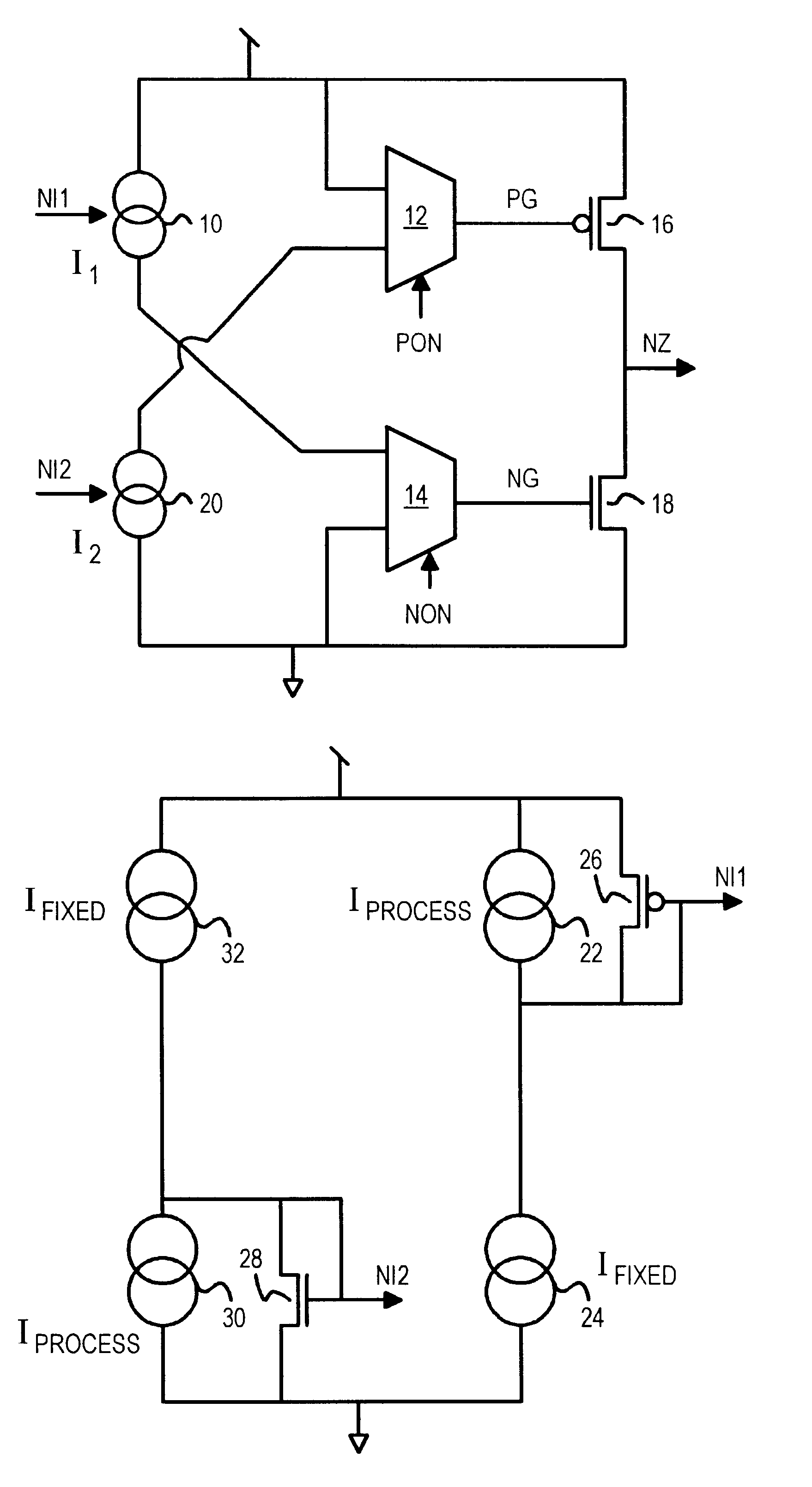
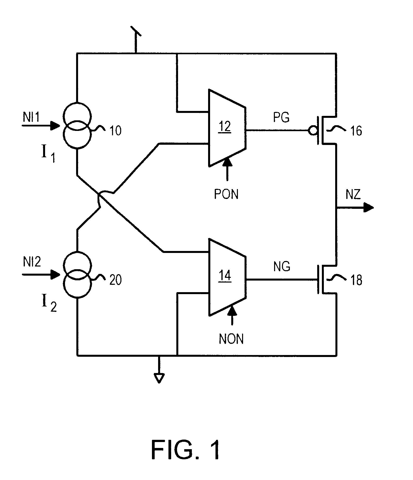
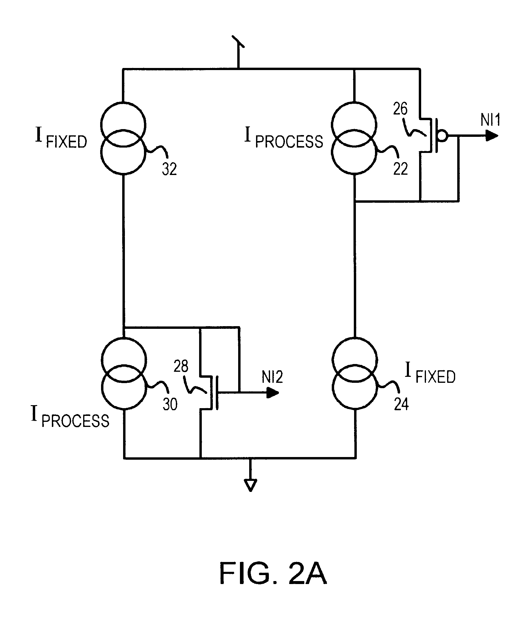
Embodiment Construction

Several other embodiments are contemplated by the inventor. For example additional devices such as capacitors, resistors, transistors, and buffer stages may be added at various locations in the circuits. Large transistors may be split into two or more smaller transistors, and smaller parallel transistors may be combined into a larger transistor. Multi-gate and stacked-gate transistors may be substituted. More current-summing networks may be added to further adjust the compensation current.

The abstract of the disclosure is provided to comply with the rules requiring an abstract, which will allow a searcher to quickly ascertain the subject matter of the technical disclosure of any patent issued from this disclosure. It is submitted with the understanding that it will not be used to interpret or limit the scope or meaning of the claims. 37 C.F.R..sctn. 1.72(b). Any advantages and benefits described may not apply to all embodiments of the invention. When the word "means" is recited in a...


PUM


Abstract

Edge rates for output driver transistors are increased for slower conditions such as caused by supply-voltage, temperature, and process variations. The edge rates are increased by increasing charging and discharging currents to the gates of the driver transistors. Process-sensing transistors have gates tied to power or ground. Current through the process-sensing transistors changes with supply-voltage, temperature, and process variations. The currents through process-sensing transistors are used to generate process-compensated voltages that bias current sources and sinks to adjust process-dependent currents. Process-independent or fixed current sources and sinks use process-independent reference voltages ultimately generated from reference currents that are not sensitive to process variations. The process-dependent-currents are subtracted from the fixed currents to produce the charging and discharging currents.

Description

BACKGROUND OF INVENTIONThis invention relates to output buffers, and more particularly to temperature, process, and voltage compensation for an output buffer.Electronic systems are often constructed from integrated circuits (IC's) using s semiconductor process technology such as a complementary metal-oxide-semiconductor (CMOS) process. CMOS processes are used construct circuits of n-channel and p-channel transistors that sink or source current.The rise and fall times of outputs of CMOS circuits are often critical parameters. When fall times are too fast, undesirable effects can occur such as ground bounce and ringing. Slow rise and fall times may be more sensitive to external noise coupled into the output. Often the rise and fall times are tightly specified to meet requirements of other circuits driven by the output.The amount of current passing through a CMOS transistor depends on several factors, such as input and output voltages, temperature, and process variations. For example, ...

Claims


Application Information

Patent Timeline
IPC IPC(8): H03K19/003
CPCH03K19/00384
Inventor WING, CHOY KWOK
Owner DIODES INC
Why Eureka
Try Eureka