Printed circuit board testing module

a printed circuit board and testing module technology, applied in the field of communication, can solve the problems of insufficient dissipation of heat generated by the pcb, the need for tests to be performed, and the difficulty of removing the pcb from the soldered connection without damaging or destroying the pcb

Inactive Publication Date: 2004-02-17
CIENA
View PDF16 Cites 12 Cited by
  • Summary
  • Abstract
  • Description
  • Claims
  • Application Information

AI Technical Summary

Problems solved by technology

Furthermore, tests need to be performed when PCBs fail in the field.
After the PCB is soldered and tested, it is difficult to remove the PCB from the soldered connections without damaging or destroying the PCB.
Unfortunately, when PCBs are removed from their assemblies and are electrically connected for testing purposes, the heat generated by the PCB is not sufficiently dissipated which increases the PCB temperature significantly.
In other words, conventional PCB fixtures fail to provide a mechanism to cool the PCB as it is being tested outside the assembly in which it normally operates.
The increased heat may damage the PCB, adding significant costs for replacement or repair of the damaged PCB.
The heat may also create latent defects in the PCB that do not surface until after the PCB is in operation.
Moreover, some PCBs have a narrow operating range such that significant deviations in temperature will affect the performance of the PCB and may lead to inaccurate testing results.

Method used


Image

  • Printed circuit board testing module
  • Printed circuit board testing module
  • Printed circuit board testing module

Examples


Embodiment Construction

The following detailed description of the invention refers to the accompanying drawings. The same reference numbers in different drawings identify the same or similar elements. Also, the to following detailed description does not limit the invention. Instead, the scope of the invention is defined by the appended claims and equivalents thereof.

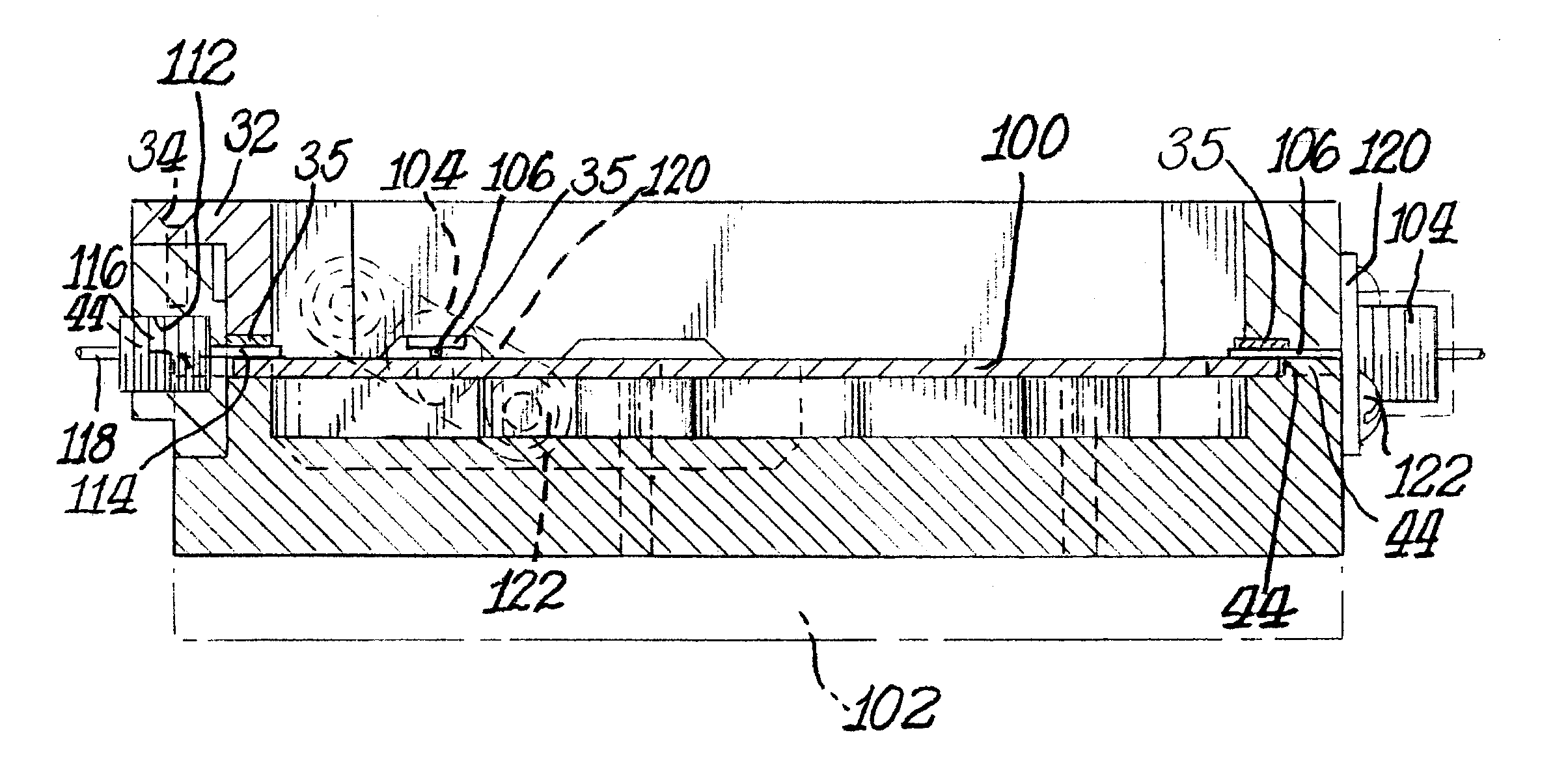
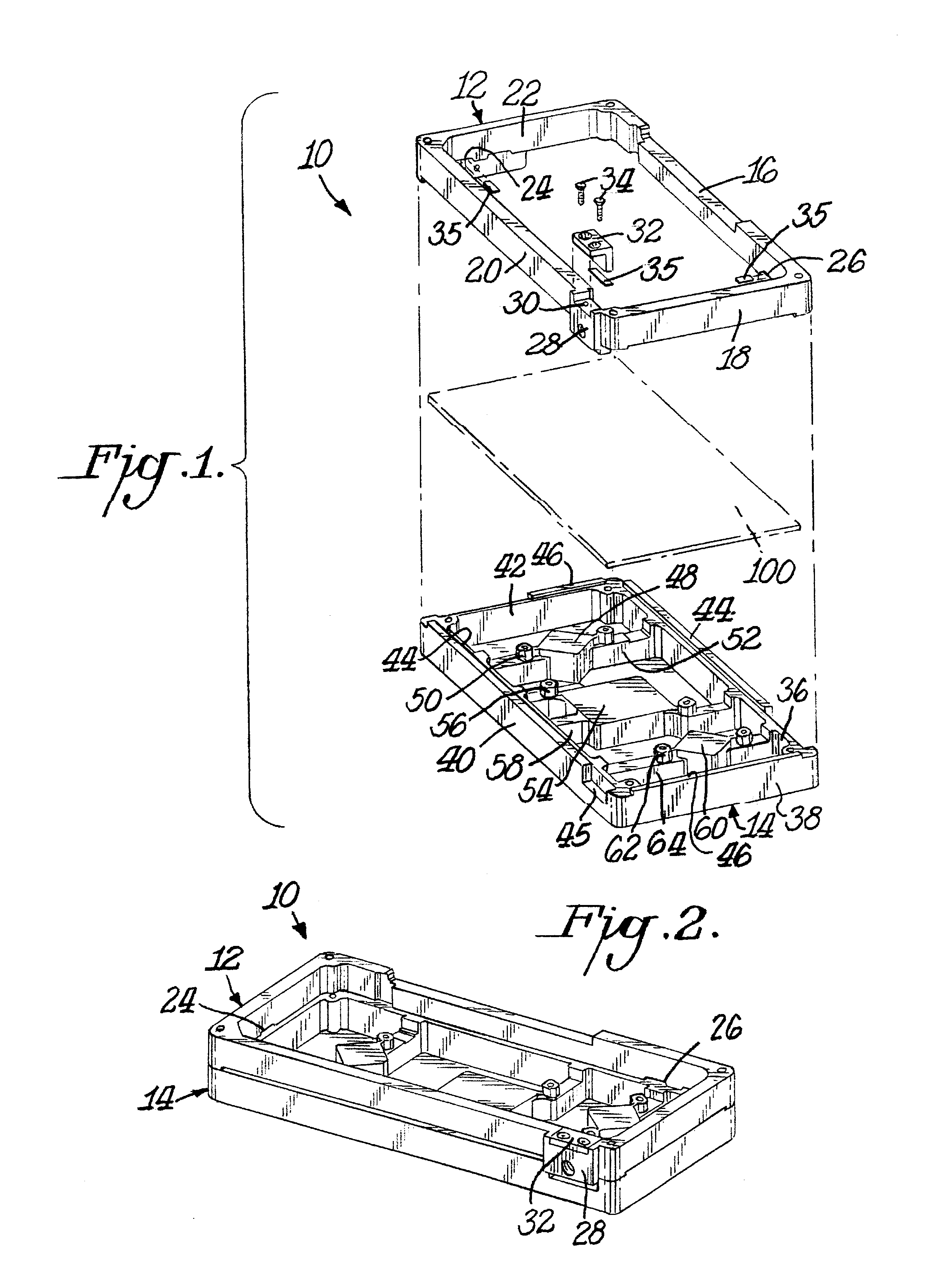
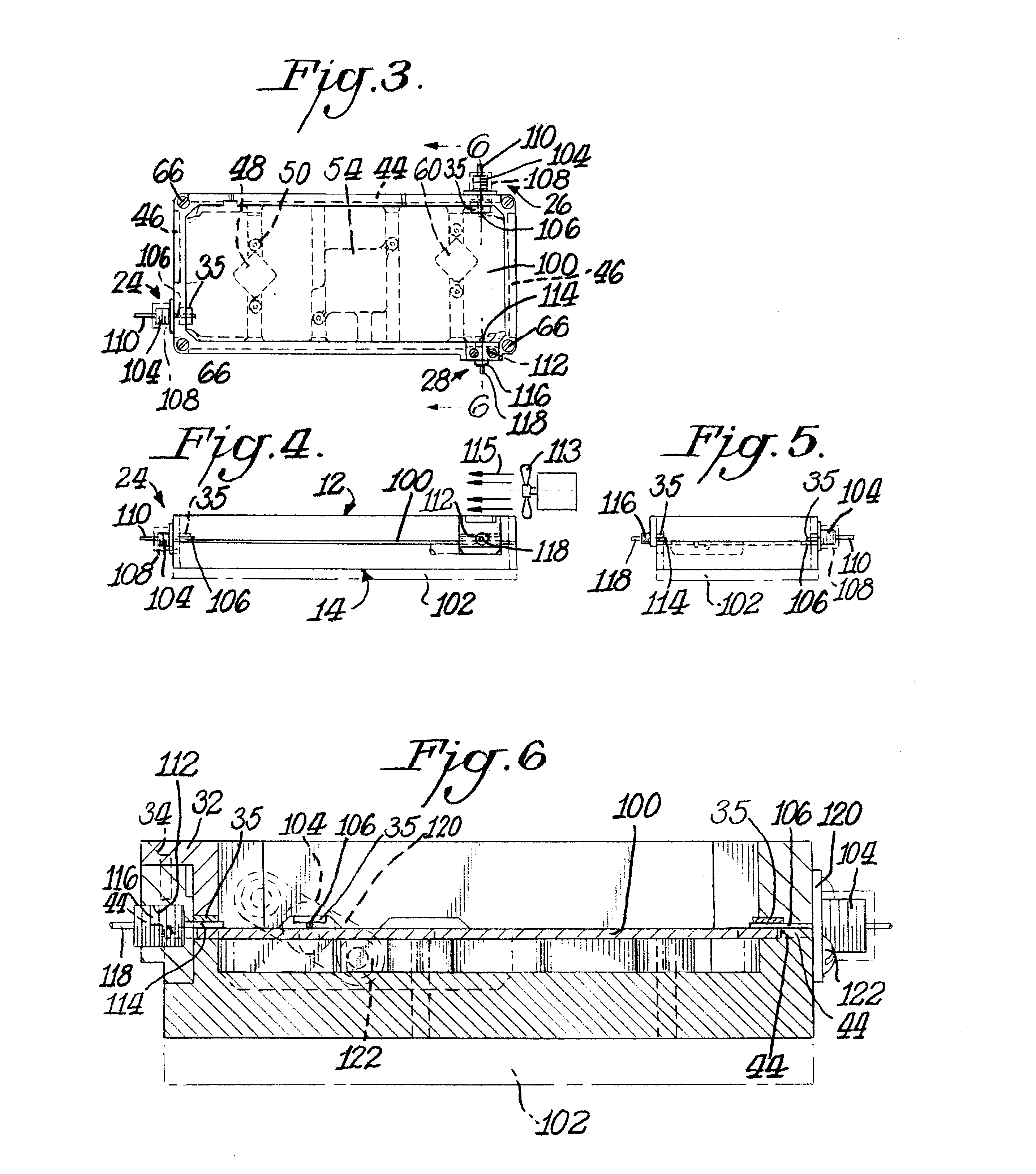
Referring now specifically to the drawings, an embodiment of the module of the present invention is illustrated in FIGS. 1-6, and shown generally as reference numeral 10. As shown in FIGS. 1 and 2, module 10 includes a top bracket 12 and bottom bracket 14 that retain a printed circuit board (PCB) 100 therebetween. Top and bottom brackets 12, 14 are substantially open to permit access to the components mounted on both the top and bottom of PCB 100. Thus, module 10 may be used with PCBs having components mounted on the top of the PCB, the bottom, or both.

Top bracket 12 may be a variety of shapes, depending upon the shape of the PCB 100. In this e...


PUM


Abstract

A module for holding a printed circuit board (PCB) includes rectangular-shaped, mating top and bottom brackets. Three walls of the top bracket retain SMA connectors that interconnect with the PCB. A dielectric gasket is provided below each SMA connector to provide pressure on the leads thereof so that the leads adequately contact corresponding pads on the PCB. Two walls of the bottom bracket include channels that slidably receive and retain the PCB therein, and another wall includes a stop channel that retains an edge portion of the PCB when the PCB is slid through the channels. The bottom bracket also has diamond-shaped pads and a square-shaped pad connected between two walls thereof that align with and support corresponding components provided on the PCB and dissipate heat generated thereby. A cable connector provided on one end of an electrical cable connects to each SMA connector, and the other ends of the electrical cables connect to testing equipment. Thus, when the top bracket is connected to the bottom bracket, the dielectric gaskets provide pressure on SMA connector leads so that the leads adequately contact corresponding pads on the PCB and enable the PCB to be tested without being permanently affixed to the module. The module may be attached to a heatsink that, in conjunction with the diamond-shaped pads and the square-shaped pad, permits heat to be dissipated from the PCB at the same rate that heat is dissipated from an installed PCB.

Description

A. Field of the InventionThe present invention relates generally to the communications field, and, more particularly to a module for holding printed circuit boards (PCB) used in the communications field.B. Description of the Related ArtPrinted circuit board (PCB) assemblies are used in computers, communications equipment, televisions, and many other products. In a typical PCB assembly, many electrical components are attached to the top and bottom surfaces of a PCB. Since the electronics manufacturing industry is highly competitive, it is important to maximize the throughput of processing PCB assemblies and to securely attach functional electrical components to the PCBs.The manufacturing of PCB assemblies involves many processes, one of which is surface mounting components to PCBs. In addition to maximizing the throughput of processing PCB assemblies, it is also becoming important to accurately mount a large number of very small components to one side of the PCB assemblies. Once the ...

Claims


Application Information

Patent Timeline
Patent Type & Authority Patents(United States)
IPC IPC(8): G01R31/28H01R13/00H01R13/646
CPCG01R31/2808H01R24/50H01R2103/00
Inventor SCHMUKLER, JOSEPH A.CYMEK, DEAN MICHAELDAR, IQBAL
Owner CIENA
Why Eureka
Try Eureka