Method of preparing optically imaged high performance photomasks

a high-performance, optical image technology, applied in the direction of photomechanical treatment originals, photomechanical instruments, photomechanical equipment, etc., can solve the problems of difficult to do the metrology which is used to determine whether the finished reticle is finished or no

Inactive Publication Date: 2004-03-09
APPLIED MATERIALS INC
View PDF31 Cites 27 Cited by
  • Summary
  • Abstract
  • Description
  • Claims
  • Application Information

AI Technical Summary

Problems solved by technology

Various efforts are made within the industry to improve the reliability of manufacturing processes by improving individual process steps; however, when a production process involves a number of interrelated process steps, alteration of an individual process step may have an unexpected result on other interrelated process steps.
As disclosed in the '859 application, there are a number of problems encountered in trying to produce a photomask / reticle when the photomask pattern exhibits critical dimensions of less than 0.3 .mu.m.
The foot is not uniform in size across the reticle substrate surface because the basisity changes somewhat randomly across the substrate surface.
Since the foot is variable, it makes it difficult to do the metrology which is used to determine whether the finished reticle will meet dimensional requirements.
However, they discovered that pattern profile abnormalities appear which limit the use of a negative resist.
Fissures as thick as 0.1 to 0.2 .mu.m were observed in the pattern at the interface with the substrate, resulting in a loss of adhesion in fine patterns.
The problem was observed for resists imaged and developed on both spin on glass (SOG) and aluminum substrates.
However, the high acceleration voltage lowers the sensitivity of resists.
However, many of the problems described above are experienced in producing a reticle using an optical imaging system in combination with a chemically amplified photoresist.

Method used


Image

  • Method of preparing optically imaged high performance photomasks
  • Method of preparing optically imaged high performance photomasks
  • Method of preparing optically imaged high performance photomasks

Examples


example one

FIG. 11A shows a starting structure 1100 used in the fabrication of a photomask, hereafter referred to as a reticle. In this Example, starting structure 1100 was a stack of layers (not shown to scale) which included, from top to bottom, a 5,000 .ANG. thick layer 1108 of a chemically amplified DUV photoresist, DX1100 (available from AZ Clariant Corp. of Somerville, N.J.); a 470 .ANG. thick layer 1106 of an organic ARC identified as KRF 17G (available from AZ / Clariant); a 250 .ANG. thick layer 1105 of chromium oxynitride inorganic ARC; a 750 .ANG. thick layer 1104 of chrome mask material; and a silicon oxide-containing substrate 1102.

In particular, the chemically amplified DUV photoresist, DX1100, comprises propylene glycol monomethyl ether acetate (PGMEA); PMA; 1-methoxy-2-propyl acetate; modified phenolic polymer; and an onium salt metal halide complex as a chemical amplifier. This DUV photoresist is applied over the surface of underlying organic ARC layer 1106 in the manner describ...

example two

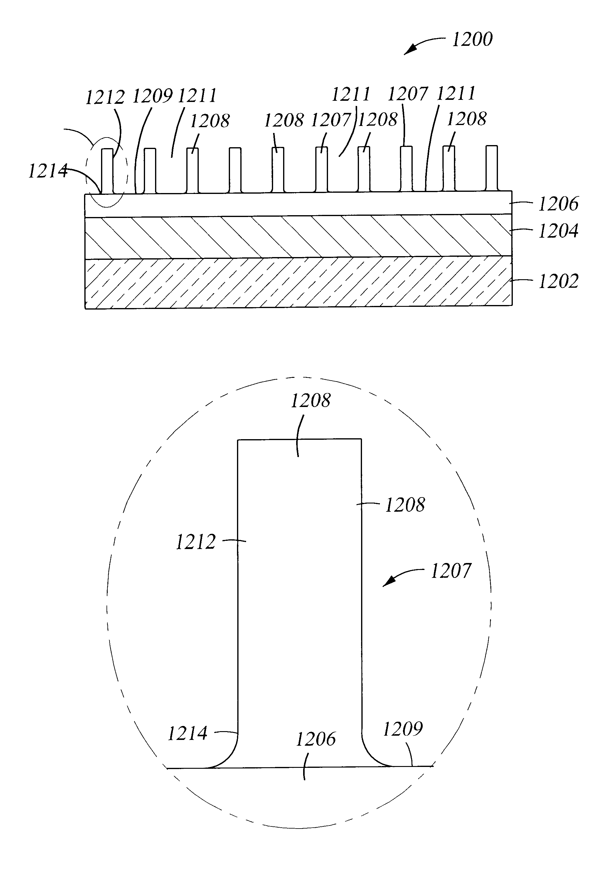
FIG. 12A shows a starting structure 1200 used in the fabrication of a photomask (reticle). In this Example, starting structure 1200 is a stack of layers which included, from top to bottom, a 5,000 .ANG. thick layer 1208 of the chemically amplified DUV photoresist, DX1100; a 540 .ANG. thick layer 1206 of the organic ARC KRF 17G; a 750 .ANG. thick layer 1204 of a mask material which is essentially chrome; and a silicon oxide-containing substrate 1202.

FIG. 12B shows a schematic cross-sectional view of the patterned photoresist layer 1208 (prior to transfer of the pattern through underlying organic ARC layer 1206, and chrome-containing layer 1204), where the pattern is lines 1207 and spaces 1211, where the line width is about 0.30 .mu.m and the spacing between lines is about 0.3 .mu.m. The patterning is done using the direct write continuous wave laser, in particular, the 257 nm mask writing laser tool available from ETEC Systems which was described above. The patterning method is as de...

example three

During the development of correlations between the PAB and PEB and critical dimension sensitivity and uniformity, applicants discovered that an increased shelf life can be obtained for photoresist coated photomask / reticle substrates prior to imaging (prior to exposure to radiation for patterning). An increased shelf life for these photoresist coated substrates is particularly important, since the manufacturer for the coated substrates is typically not the same as the manufacturer who exposes the coated substrates to radiation to create an image in the photoresist.

FIG. 3 shows a graph 300 of the critical dimension in nm obtained in chrome when a photoresist-coated (193 nm chemically amplified photoresist from Tokyo Ohka America, having offices in Hillsboro, Oreg.) photomask substrate was stored in ambient atmosphere in a clean room at room temperature prior to exposure to radiation for imaging. The PAB used after application of the photoresist was 90.degree. C. for 60 seconds. Imagin...


PUM

PropertyMeasurementUnit
temperatureaaaaaaaaaa
wavelengthaaaaaaaaaa

Abstract

One principal embodiment of the disclosure pertains to a method of optically fabricating a photomask using a direct write continuous wave laser, comprising a series of steps including: applying an organic antireflection coating over a surface of a photomask which includes a chrome-containing layer; applying a chemically-amplified DUV photoresist over the organic antireflection coating; post apply baking the DUV photoresist over a specific temperature range; exposing a surface of the DUV photoresist to the direct write continuous wave laser; and, post exposure baking the imaged DUV photoresist over a specific temperature range. The direct write continuous wave laser preferably operates at a wavelength of 244 nm or 257 nm. In an alternative embodiment, the organic antireflection coating may be applied over an inorganic antireflection coating which overlies the chrome containing layer.

Description

In general, the present invention relates to a method of producing a lithographic mask (reticle) for use in the semiconductor industry. In particular, the invention pertains to a particular combination of process steps useful in preparing optically imaged high performance photomasks. The optical imaging of the photomask makes use of a deep ultraviolet (DUV) photoresist in combination with at least one antireflective coating (ARC). The DUV photoresist is imaged using an optical direct write continuous laser mask writing tool.BRIEF DESCRIPTION OF THE BACKGROUND ARTPhotoresist compositions are used in microlithographic processes for making miniaturized electronic components, such as in the fabrication of semiconductor device structures. The miniaturized electronic device structure patterns are typically created by transferring a pattern from a patterned masking layer overlying the semiconductor substrate rather than by direct write on the semiconductor substrate, because of the time ec...

Claims


Application Information

Patent Timeline
Patent Type & Authority Patents(United States)
IPC IPC(8): G03F1/08G03F7/16G03F7/09G03F7/038G03F1/46G03F1/68G03F7/039G03F7/11G03F7/20G03F7/38H01L21/027
CPCG03F1/46G03F1/68G03F7/168G03F7/091G03F7/2051Y10S430/146Y10S430/151G03F1/50G03F1/76G03F7/00
Inventor FULLER, SCOTTMONTGOMERY, MELVIN W.ALBELO, JEFFREY A.BUXBAUM, ALEX
Owner APPLIED MATERIALS INC
Why Eureka
Try Eureka