

Through-pad slurry delivery for chemical-mechanical polish
- Summary
- Abstract
- Description
- Claims
- Application Information
AI Technical Summary
Problems solved by technology
Method used
Image

Examples
Embodiment Construction
In the following description, numerous details, such as specific materials, dimensions, and processes, are set forth in order to provide a thorough understanding of the present invention. However, one skilled in the art will realize that the invention may be practiced without these particular details. In other instances, well-known semiconductor equipment and processes have not been described in particular detail so as to avoid obscuring the present invention.
Various embodiments of an apparatus for and a method of delivering a slurry through a pad for a chemical-mechanical polish (CMP) process according to the present invention will be described.
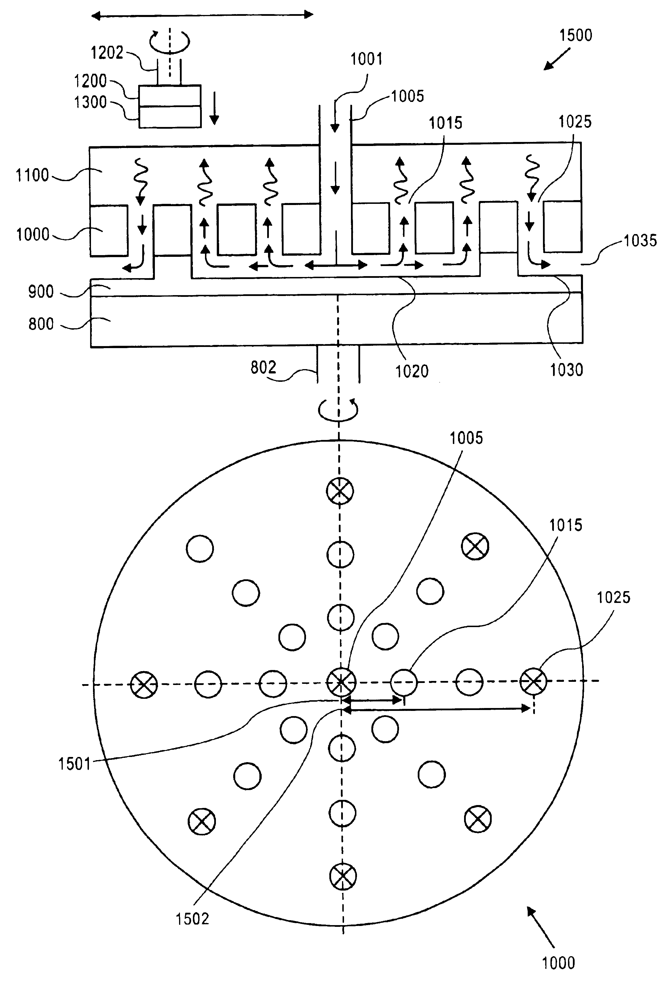
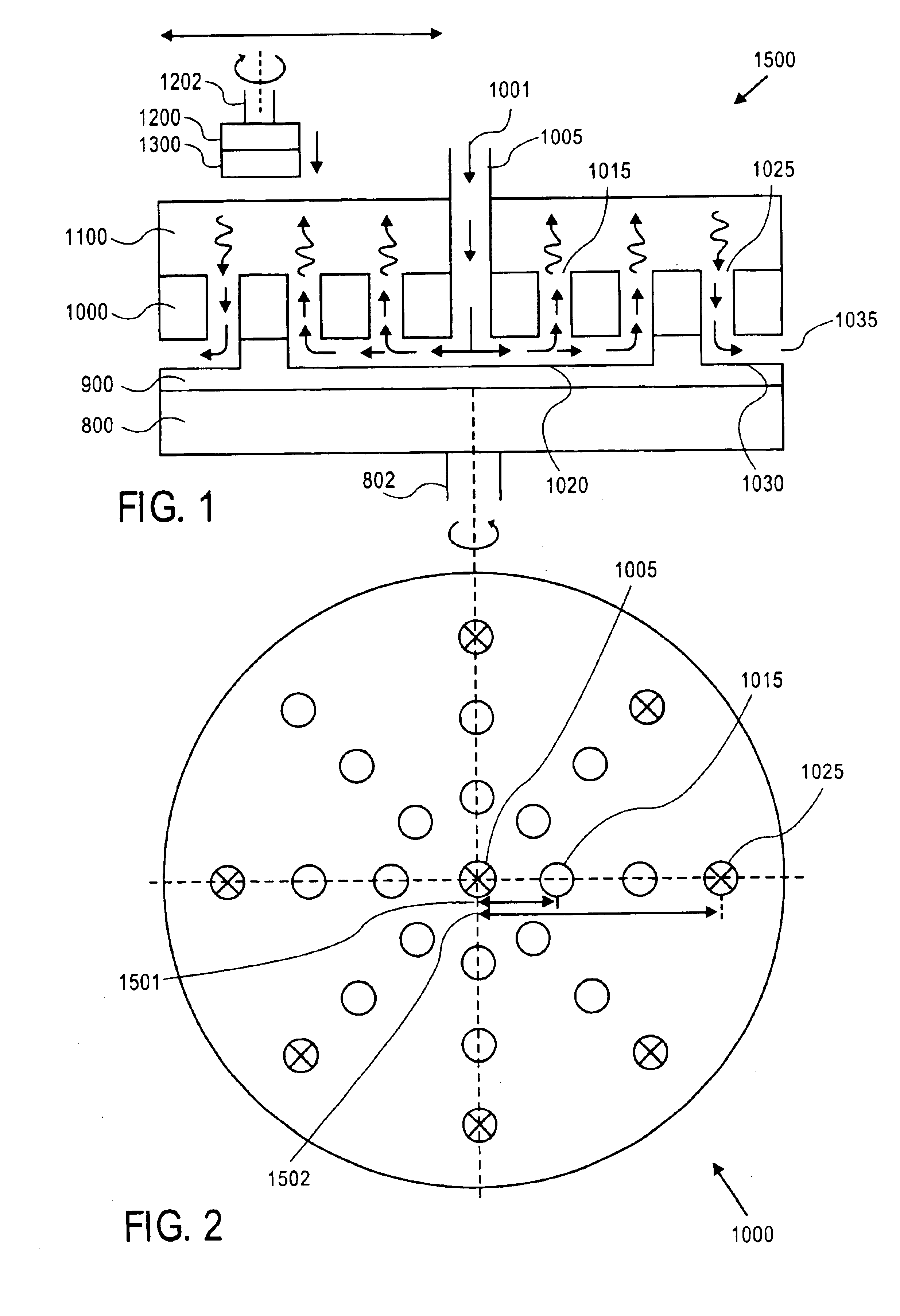
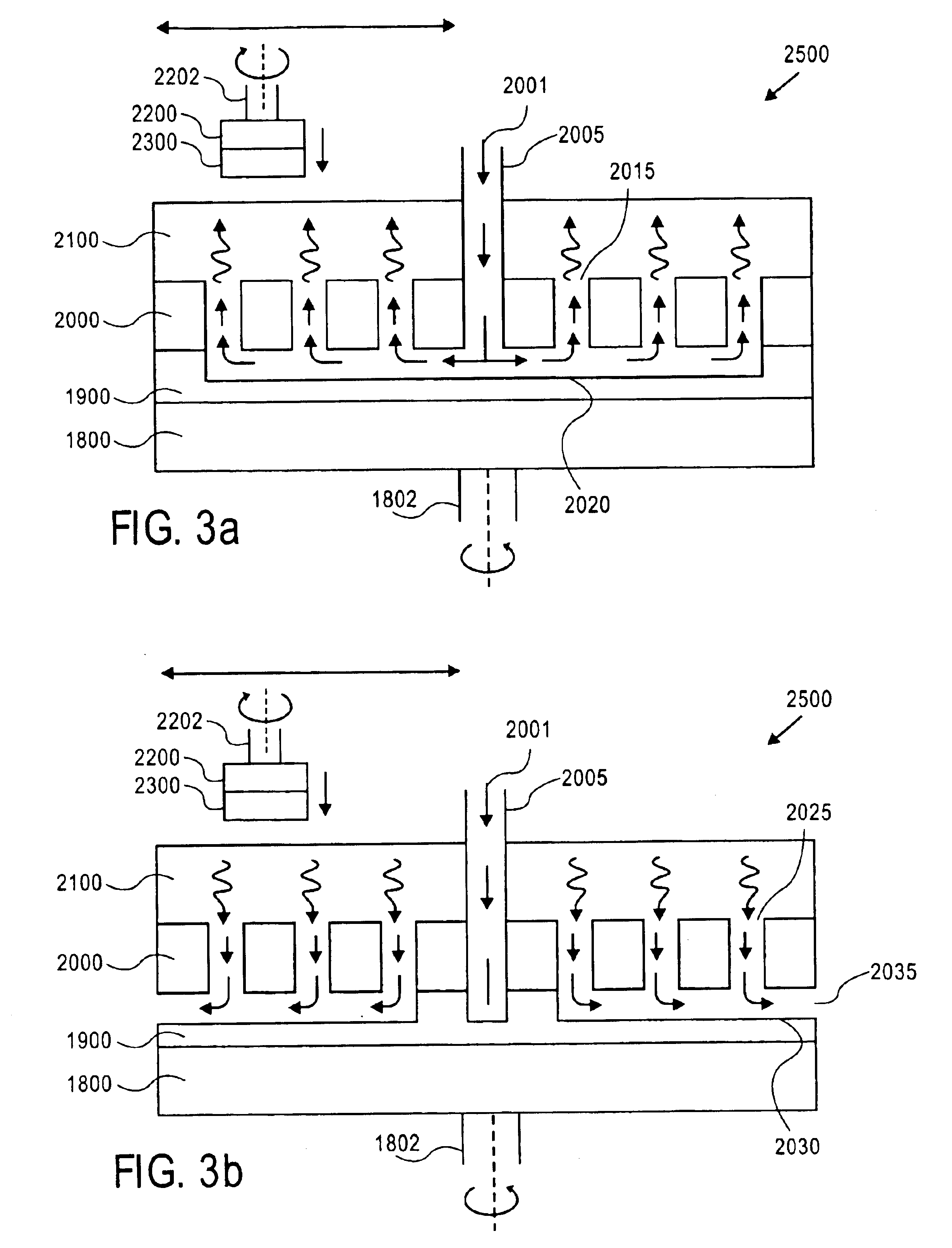
FIG. 1 is an illustration of an elevation view of an embodiment of an apparatus 1500 for delivering a slurry 1001 through a polish pad 1100 for CMP according to the present invention. A substrate 1300 may be held by a carrier 1200 on a head. The polish pad 1100 may be connected or coupled, through a vertical distribution layer 1000 and a lat...
PUM
| Property | Measurement | Unit |
|---|---|---|
| Centrifugal force | aaaaa | aaaaa |
| Distribution | aaaaa | aaaaa |
Abstract
Description
Claims
Application Information