Dynamic lot allocation based upon wafer state characteristics, and system for accomplishing same

a technology of dynamic lot allocation and wafer state characteristics, applied in the direction of manufacturing tools, grinding machine components, testing/measurement of semiconductor/solid-state devices, etc., can solve the problems of adverse impact on subsequent processing, device yield and overall manufacturing efficiency, and difficulty in maintaining feature size accuracy in other areas

Inactive Publication Date: 2004-06-08
GLOBALFOUNDRIES INC
View PDF9 Cites 250 Cited by
  • Summary
  • Abstract
  • Description
  • Claims
  • Application Information

AI Technical Summary

Problems solved by technology

All of these variations can have an adverse impact on subsequent processing, device yields and overall manufacturing efficiencies.
As a result, the additional etch time required to etch through the additional thickness of the process layer may damage the underlying process layers, and / or cause difficulty in maintaining feature size accuracy in other areas of the process layer.
As a result, subsequent exposure processes performed in a stepper tool may be adversely impacted.
For example, given the variation in photoresist thickness, there may be unacceptable deviations in the critical dimension of photoresist features formed in areas of the layer of photoresist having different thicknesses.
Such methodologies may, in some cases, require extensive capital, material and labor to implement, and they may not be necessary or appropriate for some semiconductor manufacturing operations.
Moreover, it will be appreciated that such a development effort might be complex and time-consuming, but would nevertheless be a routine undertaking for those of ordinary skill in the art having the benefit of this disclosure.
Without more, the variations in the critical dimensions of the gate electrodes 16 would result in devices having different, and perhaps unacceptable, electrical performance characteristics, i.e., some of the device will have too low of an operating speed or exhibit off-state leakage currents that are too large.
Nevertheless, the wafers with differing characteristics remained in their original lot and were subjected to additional processing on the assumption that any variations were unimportant.

Method used


Image

  • Dynamic lot allocation based upon wafer state characteristics, and system for accomplishing same
  • Dynamic lot allocation based upon wafer state characteristics, and system for accomplishing same
  • Dynamic lot allocation based upon wafer state characteristics, and system for accomplishing same

Examples


Embodiment Construction

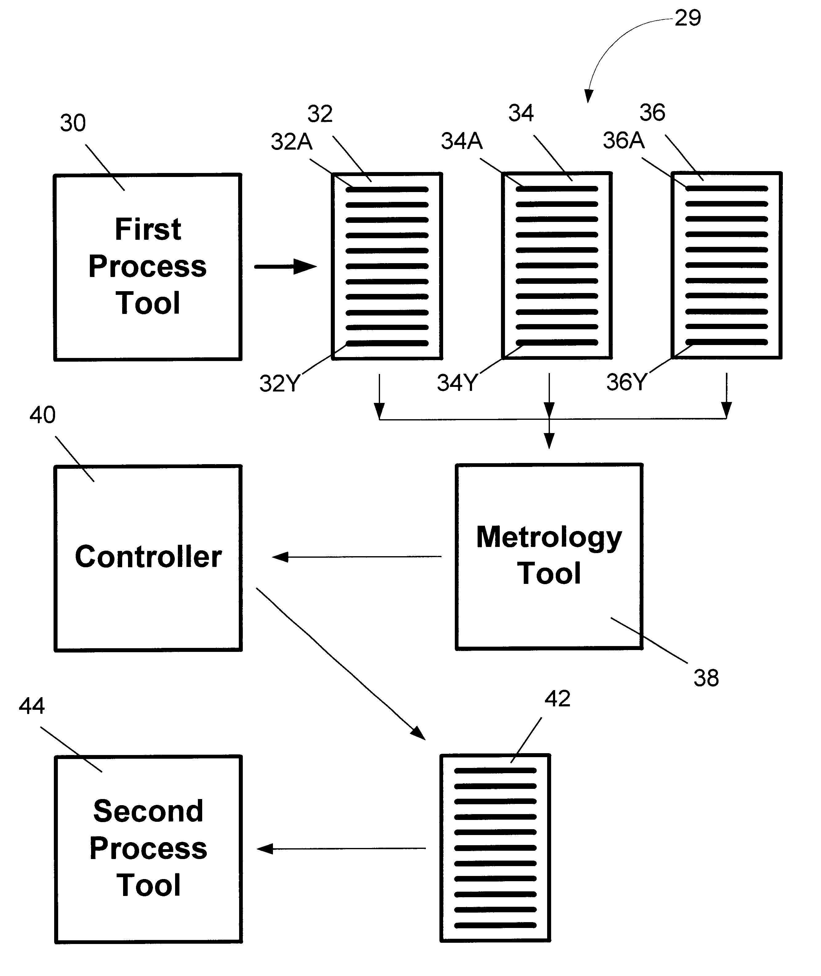
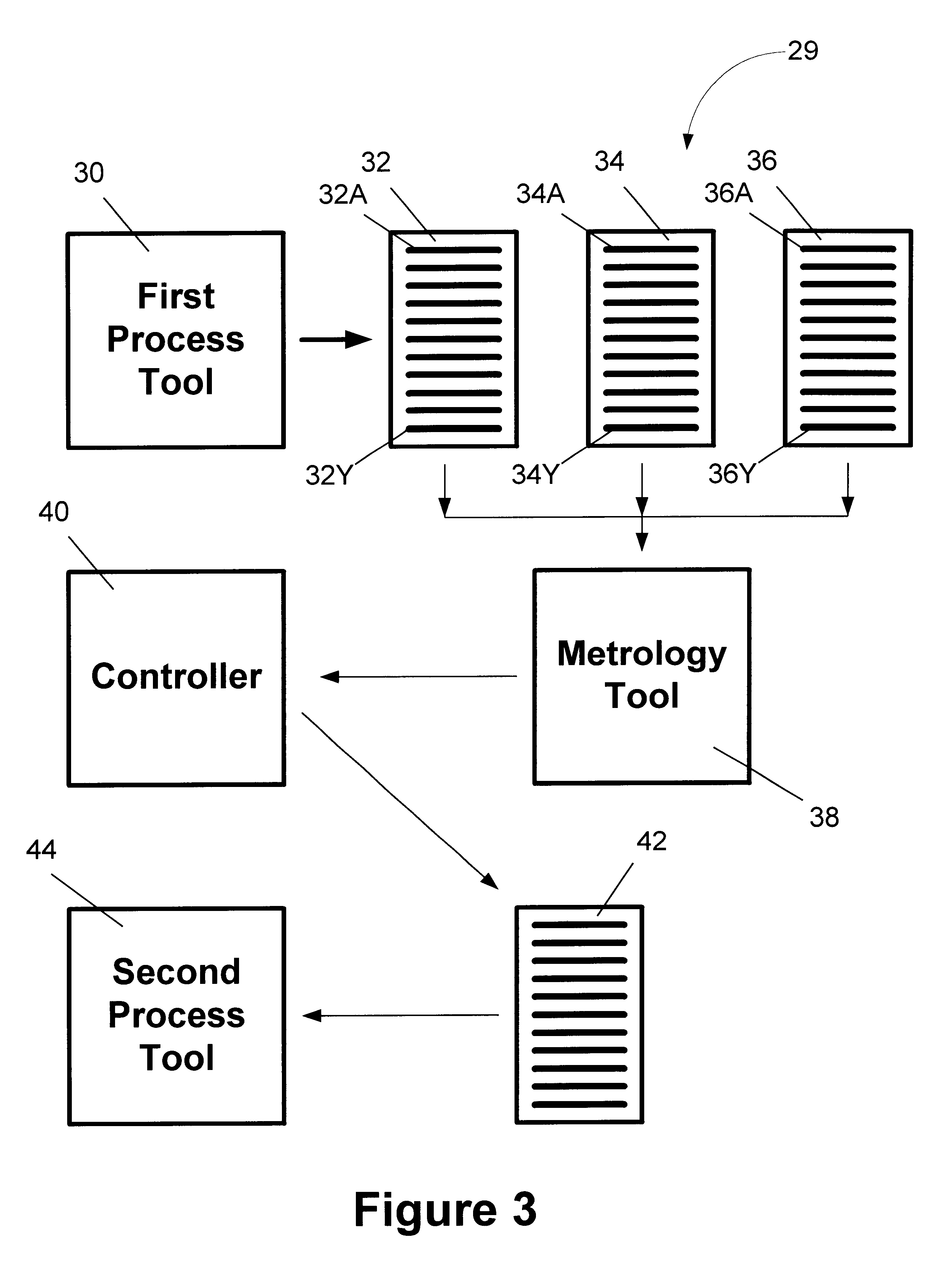
, the processing operations performed on the wafers before and / or after the lot re-allocation of the present invention may be comprised of at least one of an etching process operation, a deposition process operation, a chemical mechanical polishing process, an ion implant process operation, and a heating operation.

In another aspect, the present invention is directed to a system that comprises a first processing tool for performing processing operations on each of a plurality of wafers in each of a plurality of wafer lots, a controller for identifying processed wafers having similar characteristics and re-allocating the wafers to lots based upon the identified characteristics, and a second processing tool adapted to perform additional processing operations on the identified wafers having similar characteristics in the re-allocated lot.

In another aspect, the present invention is directed to a system that is comprised of a first processing means for performing processing operations on ...


PUM

PropertyMeasurementUnit
sizesaaaaaaaaaa
surface topographyaaaaaaaaaa
thicknessaaaaaaaaaa

Abstract

In one illustrative embodiment, the method comprises providing a plurality of wafer lots, each of the lots comprising a plurality of wafers, performing at least one process operation on at least some of the wafers in each of the plurality of lots, identifying processed wafers having similar characteristics, re-allocating the wafers to lots based upon the identified characteristics, and performing additional processing operations on the identified wafers having similar characteristics in the re-allocated lots. In one illustrative embodiment, the system comprises a first processing tool for performing processing operations on each of a plurality of wafers in each of a plurality of wafer lots, a controller for identifying processed wafers having similar characteristics and re-allocating the wafers to lots based upon the identified characteristics, and a second processing tool adapted to perform additional processing operations on the identified wafers having similar characteristics in the re-allocated lot.

Description

1. Field of the InventionThe present invention is generally directed to the field of semiconductor manufacturing, and, more particularly, to dynamic lot allocation based upon wafer state characteristics, and a system for accomplishing same.2. Description of the Related ArtModern integrated circuit devices are comprised of millions of devices, e.g., transistors, formed above a semiconductor wafer comprised of, for example, silicon. Typically, integrated circuit devices are formed above a substrate in the shape of a flat, cylindrical wafer. Current semiconductor manufacturing operations use 8-inch diameter wafers. However, it is anticipated that 12-inch diameter wafers will be used in the immediate future. Additional increases in wafer size may also occur in the more distant future.In general, the process of forming integrated circuits involves the formation of layers or films of material, selective removal of portions of those layers, introducing dopant atoms into the substrate at pr...

Claims


Application Information

Patent Timeline
Patent Type & Authority Patents(United States)
IPC IPC(8): B24B1/00B24B49/00B24B51/00H01L21/66
CPCH01L22/20
Inventor BODE, CHRISTOPHER A.PASADYN, ALEXANDER J.
Owner GLOBALFOUNDRIES INC
Why Eureka
Try Eureka