
Semiconductor memory device and method of selecting word line thereof

a memory device and memory line technology, applied in the field of memory device and memory line selection method, can solve the problems of increasing layout area size, high power consumption, and large chip siz

Inactive Publication Date: 2004-06-08
SAMSUNG ELECTRONICS CO LTD
View PDF3 Cites 18 Cited by
  • Summary
  • Abstract
  • Description
  • Claims
  • Application Information

AI Technical Summary

Problems solved by technology

As a result, since sub word lines of the memory cell array block that have not to be selected are selected, power consumption is high.
Also, the conventional semiconductor memory device having a sub word line receives a row address before receiving a column address to perform a read operation and a write operation, and thus cannot select a sub word line of a certain memory cell array partial block in a memory cell array block.
However, the FCRAM device can greatly improve a data transmission rate but has a problem in that a chip size becomes large.
However, the RAM device can reduce power consumption but has a problem in that a layout area size is increased.

Method used


Image

  • Semiconductor memory device and method of selecting word line thereof
  • Semiconductor memory device and method of selecting word line thereof
  • Semiconductor memory device and method of selecting word line thereof

Examples


Embodiment Construction

Reference will now be made in detail to preferred embodiments of the present invention, example of which is illustrated in the accompanying drawings.

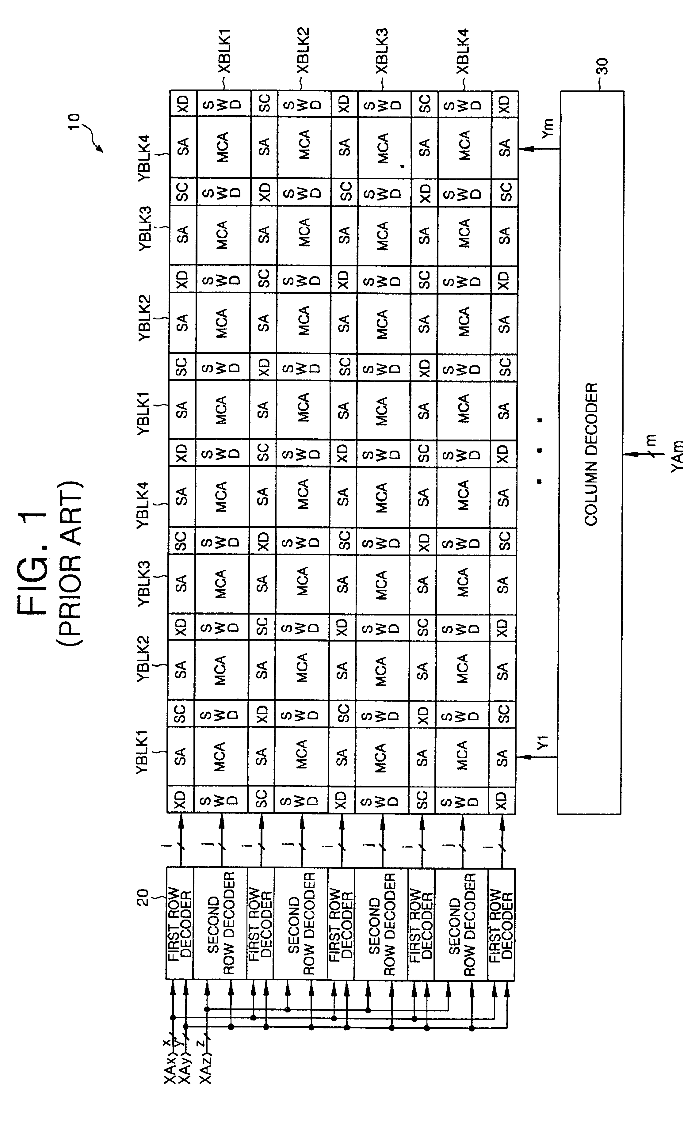
Turning now to the drawings, FIG. 1 is a block diagram illustrating a conventional semiconductor memory device having a sub word line. The semiconductor memory device of FIG. 1 includes a memory cell array 10, a row decoder 20 and a column decoder 30.

The memory cell array 10 includes memory cell array blocks XBLK1 to XBLK4, partial blocks YBLK1 to YBLK4 of respective memory cell array blocks XBLK1 to XBLK4, sub word line drivers SWD arranged on right and left sides of the partial blocks YBLK1 to YBLK4, bit line sense amplifiers SA arranged on upper and lower sides of the memory cell array blocks XBLK1 to XBLK4, and drivers XD and a sensing enable control signal generating circuit SC arranged at crossing points of the bit line sense amplifier SA and the sub word line drivers SWD. The row decoder 20 includes first and second row decoders....


PUM


Abstract

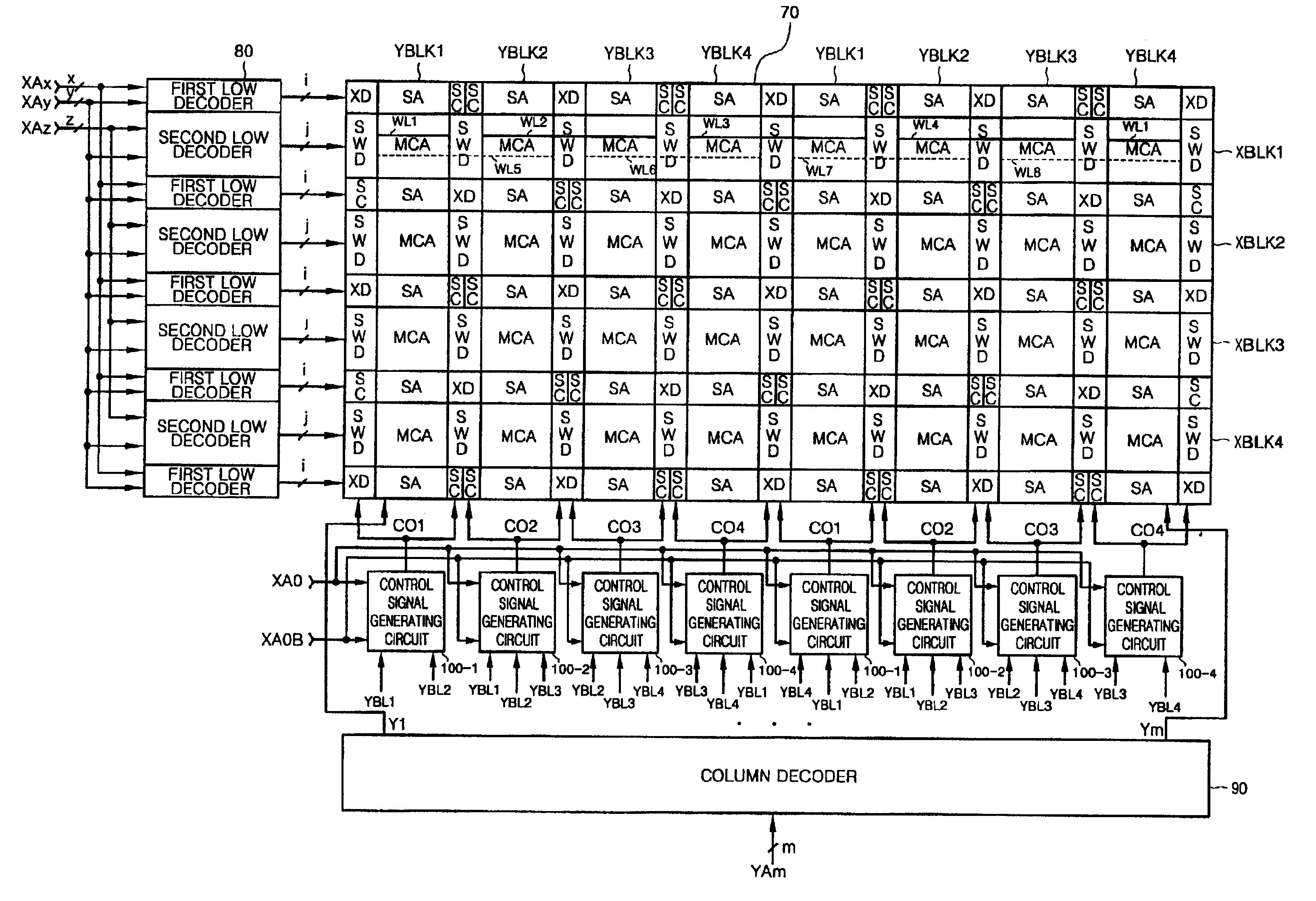
A semiconductor memory device includes a plurality of memory cell array blocks each including a plurality of partial blocks, a plurality of global word lines, and odd-numbered and even-numbered sub word lines corresponding to each of the plurality of the global word lines, the odd-numbered sub word lines of each of odd-numbered partial blocks among the plurality of the partial blocks, respectively, connected to the odd-numbered sub word lines of each of the previous neighboring partial blocks, the even-numbered sub word lines of each of the odd-numbered partial blocks among the plurality of the partial blocks, respectively, connected to the even-numbered sub word lines of each of the next neighboring partial blocks, the odd-numbered sub word lines of each of even-numbered partial blocks among the plurality of the partial blocks, respectively, connected to the odd-numbered sub word lines of each of the next neighboring partial blocks, the even-numbered sub word lines of each of the even-numbered partial blocks among the plurality of the partial blocks, respectively, connected to the even-numbered sub word lines of each of the previous neighboring partial blocks; and a control means for selecting sub word lines of a corresponding partial block and sub word lines of a neighboring partial block connected to the sub word lines of the corresponding partial block when the corresponding partial block is selected in response to externally applied row and column address.

Description

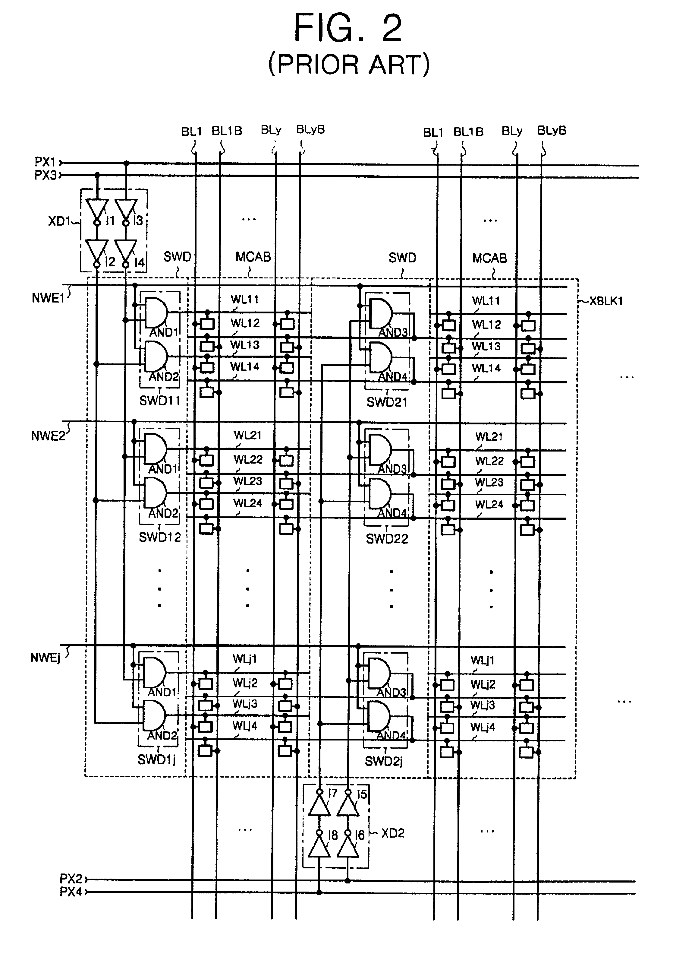
1. Field of the InventionThe present invention relates to a semiconductor memory device and a method of selecting a word line thereof.2. Description of Related ArtA conventional semiconductor memory device having a sub word line includes a plurality of memory blocks. In such a semiconductor memory device, when a row address is input in response to a row address strobe signal, one global word line is selected. When one global word line is selected, among a plurality of sub word lines, one sub word line corresponding to the selected global word line is selected. And, when a column address is input in response to a column address strobe signal, a bit line pair is selected. At this time, a selected memory cell in one memory cell array block receives or outputs a data. In other words, in the conventional semiconductor memory device having a sub word line, when one sub word line in one memory cell array block is selected, sub word lines of all partial blocks that constitute the memory cel...

Claims


Application Information

Patent Timeline
IPC IPC(8): G11C8/00G11C8/14G11C8/10G11C11/401G11C11/408
CPCG11C8/10G11C8/14
Inventor LEE, CHAN-YONGLEE, JUNG-BAE
Owner SAMSUNG ELECTRONICS CO LTD
Learn More