Electrochemical method for forming an inorganic covering layer on a surface of a copper material
a technology of inorganic coating and copper material, which is applied in the direction of electrolytic coating, surface reaction electrolytic coating, anodisation, etc., can solve the problems of poor process control, long process time, and high cost of reagents, and achieves improved adherence to the copper substrate, improved mechanical properties, and fast and simple
- Summary
- Abstract
- Description
- Claims
- Application Information
AI Technical Summary
Benefits of technology
Problems solved by technology
Method used
Image
Examples
example 2
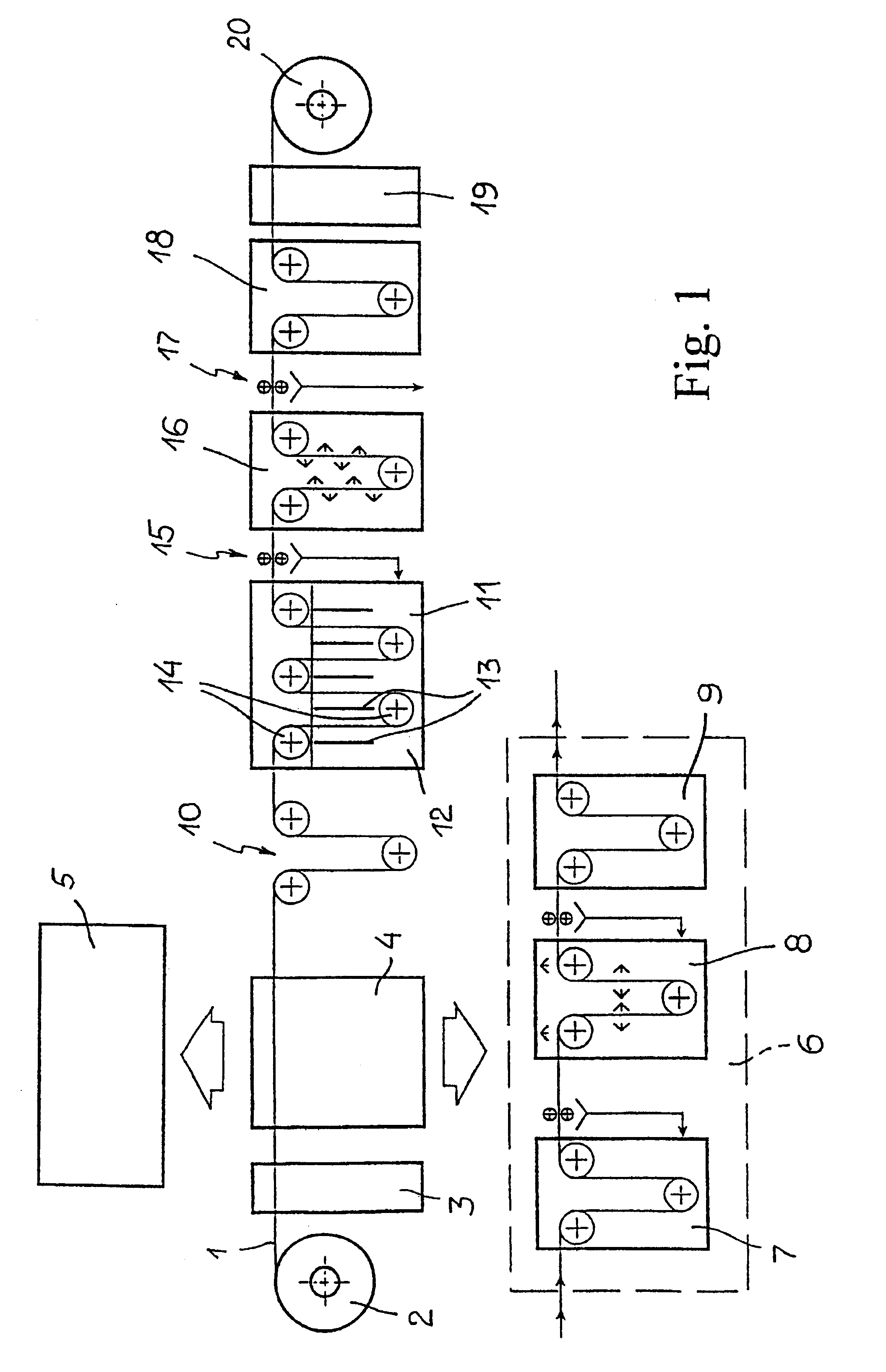
The same apparatus, cell and copper material of example 1 were used: the process and cell parameters are summarized in table II.
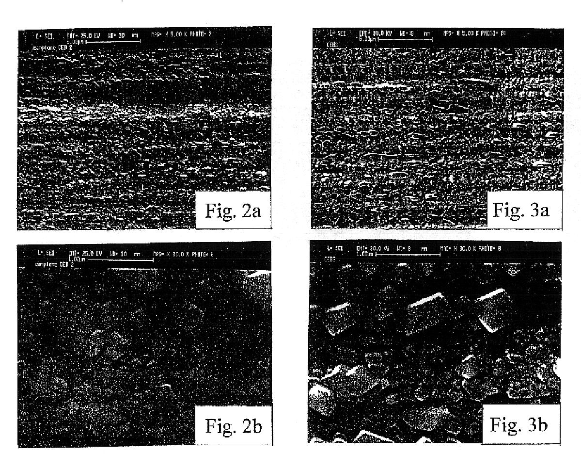
A very uniform and adherent layer was obtained (named CB3 for comparative purposes) having a brown colour.
example 3
The same apparatus, cell and copper material of example 1 were used: the process and cell parameters are summarized in table III.
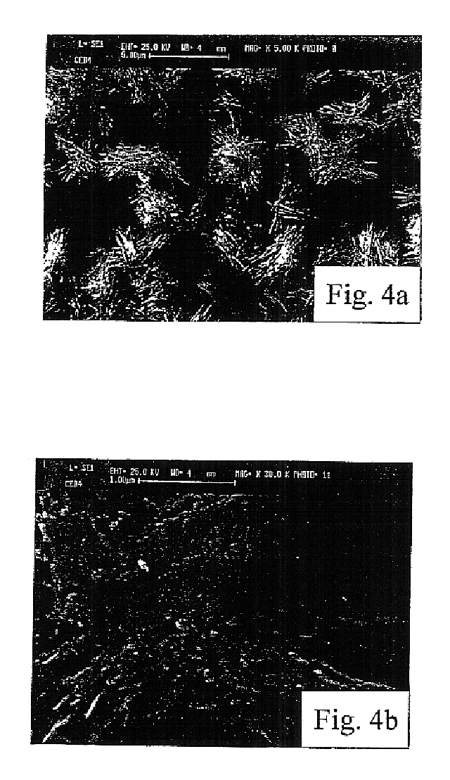
A very uniform and adherent layer was obtained (named CB4 for comparative purposes) having a deep black colour and velvety aspect.
example 4
All samples produced in the above reported examples 1 to 3 were tested for determining chemical composition (by X-ray diffractometry and coulometry), thickness (by coulometric analysis performed by reducing the superficial copper oxide, at a constant current density, in a Na.sub.2 CO.sub.3 0.1 M solution, according to the method extensively described in A. Billi, E. Marinelli, L. Pedocchi, G. Rovida: "Surface characterization and corrosion behaviour of Cu--Cu.sub.2 O--CuO system", published on the Proceedings of the 11.sup.th International Corrosion Congress, Florence, 1990, Vol. 5, p. 129, Edit Associazione Italiana di Metallurgia Milano, Italy 1990), crystalline structure (by SEM micrography and X-ray diffraction analysis): main test results are summarized in table IV.
The crystalline form of layers according to the invention is shown in FIGS. 2 to 4, which are SEM micrography pictures of the three samples CEB2, CEB3 and CEB4 respectively.
Tests were conducted for evaluating optical...
PUM
| Property | Measurement | Unit |
|---|---|---|
| current density | aaaaa | aaaaa |
| current density | aaaaa | aaaaa |
| current density | aaaaa | aaaaa |
Abstract
Description
Claims
Application Information


