Structural member superior in water repellency and method for manufacturing the same
a technology of structural members and water repellents, applied in the direction of lighting and heating apparatus, instruments, light beam reproducing, etc., can solve the problems of inferior adhesion, easy peeling of thin film, uneven film height of surface,
- Summary
- Abstract
- Description
- Claims
- Application Information
AI Technical Summary
Problems solved by technology
Method used
Image
Examples
embodiment 1
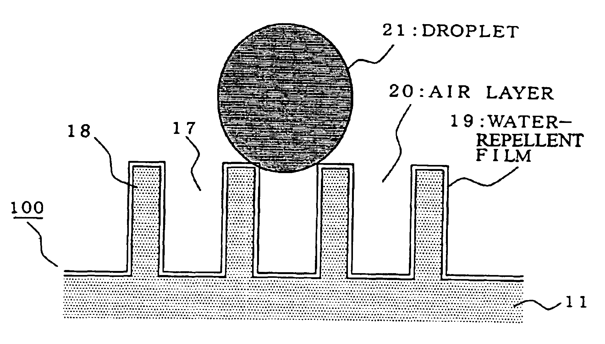
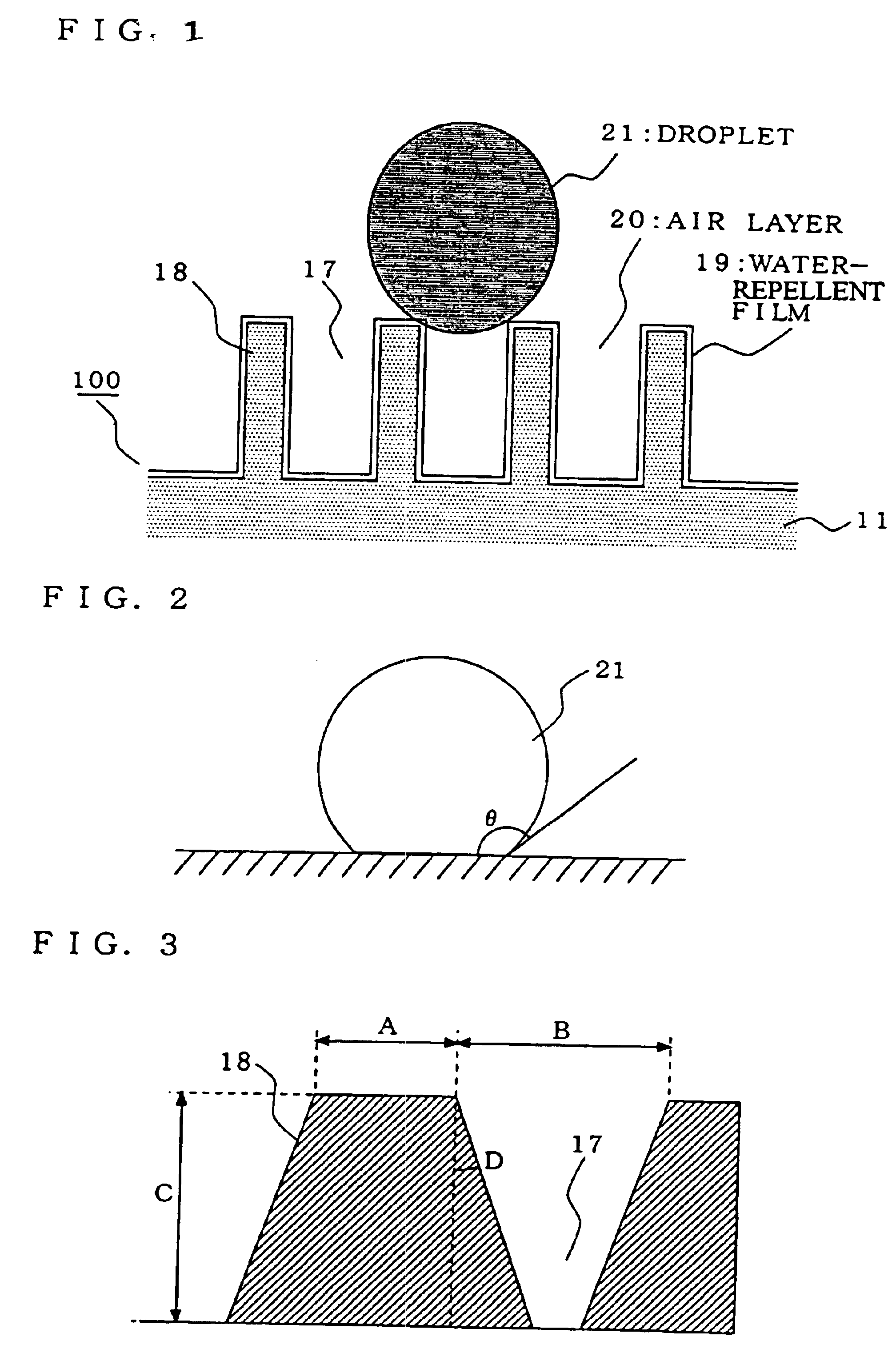
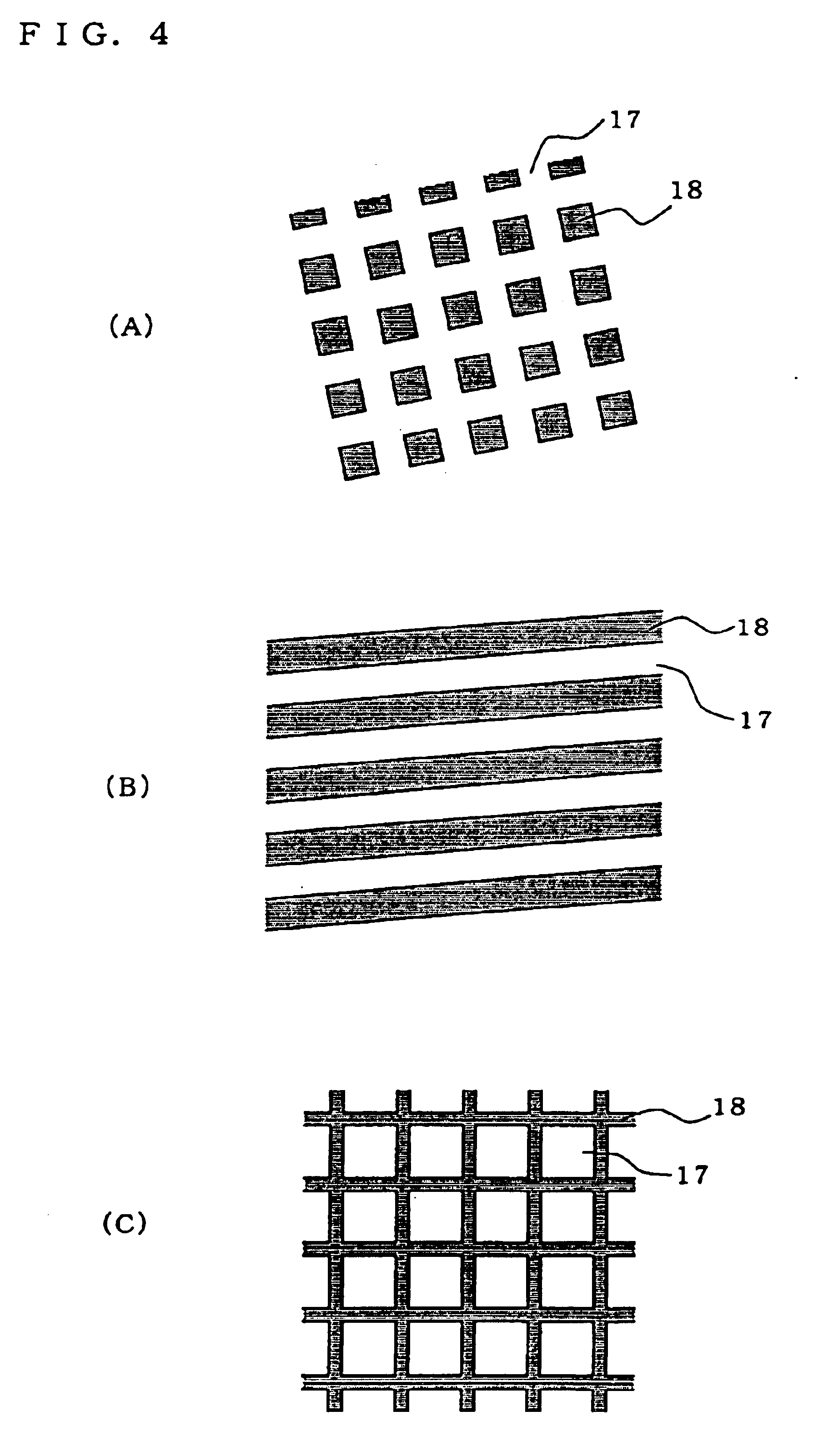
FIG. 1 is an explanatory view of a water-repellent structure according to Embodiment 1 of the present invention. In FIG. 1, in a water-repellent structure 100, recess portions 17 and protrusion portions 18 are formed on a surface of a silicon substrate 11, and a water-repellent film 19 is formed on the surfaces of the recess portions 17 and the protrusion portions 18. Air layers 20 are generated in these recess portions formed on the surface of the silicon substrate 11. Although this embodiment shows the case where the water-repellent film 19 is formed, a base material which has a water-repellent function in itself, for example, Teflon resin or the like may be used.
FIG. 2 is an explanatory view of a contact angle of water when the water-repellent function is shown. To show the water-repellent function, it is necessary that the contact angle .theta. of water is 120 degrees or more (90 degrees or more in the case of an ink droplet) as shown in FIG. 2. In order to make the contact angl...
embodiment 2
FIG. 5 is a sectional view showing a manufacturing process for forming a water-repellent structure on a surface of a plate. FIG. 6 is a top view of the plate 1 in which the water-repellent structure has been formed on the surface. The procedure of manufacturing the water-repellent structure will be described with reference to FIGS. 5 and 6. Here, description will be made about the case where the surface of a silicon substrate is worked by a photolithography method and a trench dry etching method so as to form a water-repellent structure.
1 First, a 4-inch single-crystal silicon wafer of the (100) crystal orientation is prepared as a base material of the plate 1. A silicon oxide film 12 of about 1,000 Angstroms is formed on at least one surface of the single-crystal silicon substrate 11 by use of a thermal oxidation method, as shown in FIG. 5(a).
2 Next, as shown in FIG. 5(b), about 2 ml of photosensitive resin OFPR-800 (viscosity: 30 cps) made by TOKYO OHKA KOGYO CO., LTD. is dropped ...
example 1
As Example 1 of the present invention, examples shown in Table 1 were attempted in the above-mentioned Embodiment 2. First, substrate materials of samples 1 to 7 are prepared for the plate substrate 11. Then, the protrusion-portion-expected areas 13 (see FIG. 5(c)) are formed by patterning squares each in a range from 0.2 .mu.m to 1,000 .mu.m. In addition, the water-repellent film 19 on the plate 1 is formed by depositing fluoroalkylsilane or polyfluoroethylene water-repellent material. This water-repellent treatment is not performed on the samples 2, 4 and 6.
PUM
| Property | Measurement | Unit |
|---|---|---|
| width | aaaaa | aaaaa |
| depth | aaaaa | aaaaa |
| depth | aaaaa | aaaaa |
Abstract
Description
Claims
Application Information


