Toughness, adhesion and smooth metal lines of porous low k dielectric interconnect structures

a low k dielectric and interconnecting technology, applied in the field of interconnecting structures, can solve the problems of poor adhesion, inability to use as the matrix of porous dielectrics, and delamination of metal lines

Inactive Publication Date: 2004-08-31
GLOBALFOUNDRIES U S INC
View PDF12 Cites 12 Cited by
  • Summary
  • Abstract
  • Description
  • Claims
  • Application Information

AI Technical Summary

Benefits of technology

It is an object of this invention to provide a porous dielectric stack with a buried RIE stop with improved toughness and adhesion that is based on a multilayer of spin coated dielectrics.
It is an object of this invention to provide a low-k dielectric plus copper interconnect structure with precise and uniform control over the copper conductor resistance that is based on a multilayer of spin coated dielectric layers, with improved toughness and adhesion and decreased line roughness.
The structures of this invention are unique in that they have an ultra-thin non-porous tough dielectric layer between the porous dielectric and the buried etch stop layer. This tough, thin non-porous dielectric layer serves several purposes: it improves toughness, adhesion and reliability of the interconnect structure. To improve adhesion, the non-porous layer is a version of the porous dielectric with a fracture toughness of greater than 0.3 MPa-m.sup.1 / 2 which will covalently bond with the porous dielectric to create one network, while increasing the surface area of contact with the etch stop layer by eliminating pores at the surface. Increased toughness is achieved by incorporating a tough material near the interface in the area of increased stress in the structure. This type of tough material does not have the necessary properties to support the very small pores required by the porous dielectric and therefore generally cannot be used as the matrix for the porous dielectric. Finally, by incorporating a non-porous dielectric layer between the etch stop layer and the porous dielectric layer, smoother lines can be achieved by eliminating pores at the bottom of the etch stop.
Thus, the present invention is directed to a metal wiring plus porous low dielectric constant (low-k) interconnect structure having improved toughness and adhesion, of the dual damascene type with a spin-on buried RIE stop. The inventive structure is comprised of: a) a multilayer of all spin-on dielectric materials which are applied sequentially in a single tool, and then cured in a single furnace cure step, and b) a plurality of patterned metal conductors within the dielectric multilayer. The improved toughness and adhesion is obtained by incorporating a thin, non-porous dielectric layer, which has a fracture toughness greater than 0.3 MPa-m.sup.1 / 2, between the porous dielectric and the etch stop, between the etch stop and the porous dielectric, or both.

Problems solved by technology

These structures undergo several processing steps including chemical mechanical polishing (CMP) of the copper, which create stresses within the dielectric stack that can lead to delamination.
Delamination can occur due to poor adhesion at the etch stop to dielectric interfaces, or within the dielectric due to decreased toughness of the porous dielectric and increased stress near the interfaces.
This type of tough material does not have the necessary properties to support the very small pores required by the porous dielectric and therefore generally cannot be used as the matrix for the porous dielectric.

Method used


Image

  • Toughness, adhesion and smooth metal lines of porous low k dielectric interconnect structures

Examples


Embodiment Construction

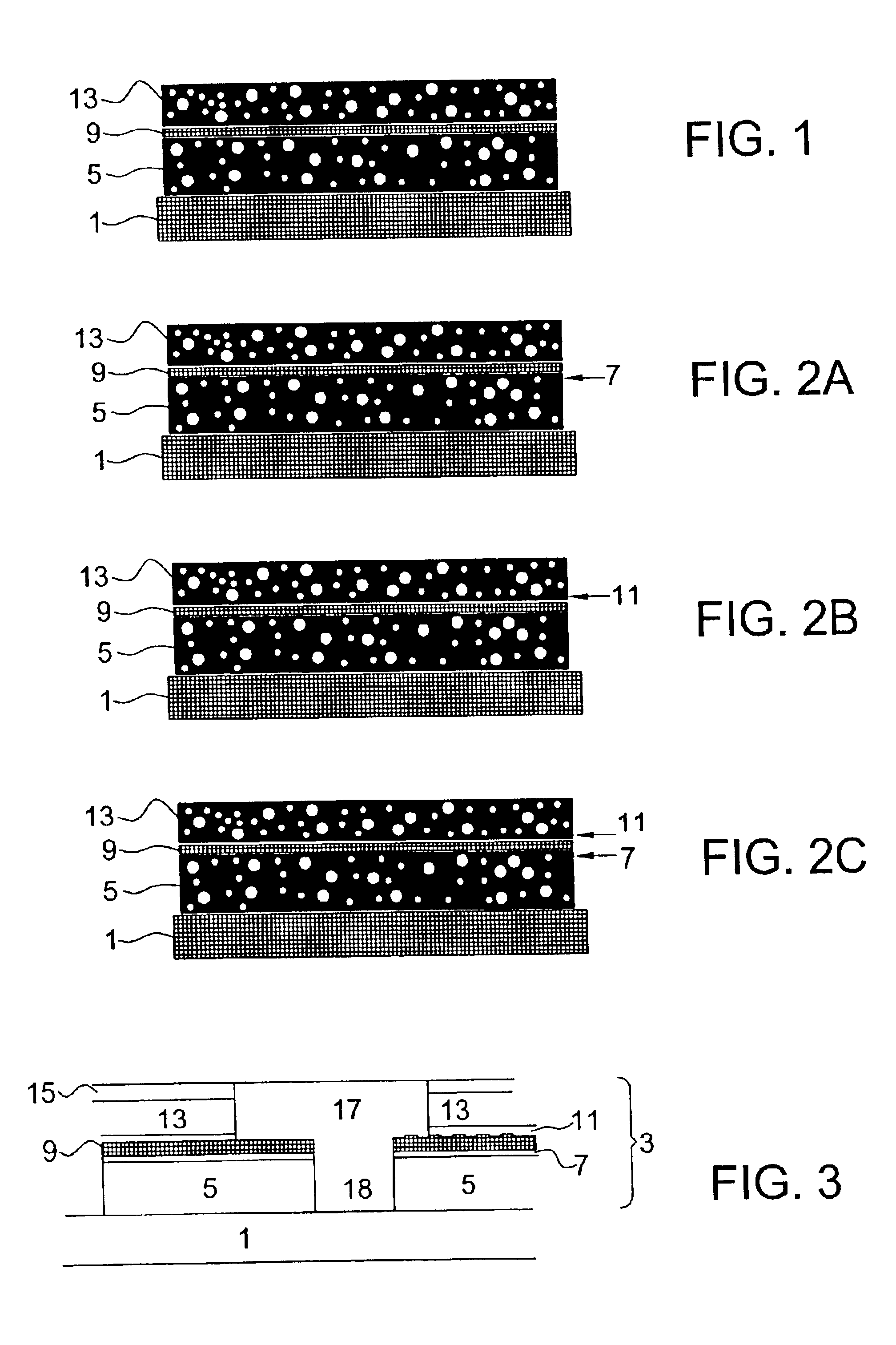
Substrate / Porous SiLK.TM. / thin SiLK.TM. layer / HOSP BESt.TM. / thin SiLK.TM. layer / Porous SiLK.TM.

FIG. 3 schematically illustrates a specific embodiment of the invention. A substrate 1 may contain transistors and an array of conductor elements. An interconnect structure 3, in accordance with the invention, is disposed on the substrate 1. Structure 3 is comprised of a first porous SiLK.TM. dielectric layer 5, having a thickness of 600-5000 Angstroms and having a highly aromatic structure which is thermally stable to approximately 425.degree. C., with a glass transition temperature above approximately 450.degree. C., and a low dielectric constant of approximately 2.2.

A thin non porous SiLK.TM. layer 7, having a fracture toughness greater than 0.30 MPa-m.sup.1 / 2 and having a thickness of approximately 25-150 Angstroms, is disposed on the first porous SiLK layer 5. As noted above, layer 7 has increased fracture toughness compared to porous SiLK due to a decreased network density. This stru...


PUM

PropertyMeasurementUnit
thicknessaaaaaaaaaa
thicknessaaaaaaaaaa
thicknessaaaaaaaaaa

Abstract

A structure useful for electrical interconnection comprises a substrate; a plurality of porous dielectric layers disposed on the substrate; an etch stop layer disposed between a first of the dielectric layers and a second of the dielectric layers; and at least one thin, tough, non-porous dielectric layer disposed between at least one of the porous dielectric layers and the etch stop layer. A method for forming the structure comprising forming a multilayer stack of porous dielectric layers on the substrate, the stack including the plurality of porous dielectric layers, and forming a plurality of patterned metal conductors within the multilayer stack. Curing of the multilayer dielectric stack may be in a single cure step in a furnace. The application and hot plate baking of the individual layers of the multi layer dielectric stack may be accomplished in a single spin-coat tool, without being removed, to fully cure the stack until all dielectric layers have been deposited.

Description

1. Field of the InventionThis invention relates to interconnect structures for high-speed microprocessors, application specific integrated circuits (ASICs), and other high speed IC's. The invention provides ultra low dielectric constant (low-k) interconnect structures having enhanced circuit speed, precise values of conductor resistance, and improved mechanical integrity. The structures of this invention have improved toughness and adhesion along with improved control over the metal line resistance compared to conventional structures. The present invention also provides many additional advantages which shall become apparent as described below.2. Background ArtThis application is related to application Ser. No. 09 / 795,431, entitled Low-k Dielectric Interconnect Structure Comprised of a Multi Layer of Spin-On Porous Dielectrics, assigned to the same assignee as the present application, and filed on Feb. 28, 2001, the contents of which are incorporated herein by reference.Many low-k di...

Claims


Application Information

Patent Timeline
Patent Type & Authority Patents(United States)
IPC IPC(8): H01L21/02H01L23/532H01L21/70H01L23/52H01L21/316H01L21/768H01L23/522
CPCH01L21/02118H01L21/02126H01L21/022H01L21/02203H01L21/02282H01L21/02362H01L21/31695H01L21/76807H01L21/7682H01L21/76829H01L21/76832H01L21/76835H01L23/5222H01L23/5329H01L23/53295H01L21/76801H01L2924/0002H01L2221/1047Y10T428/31663H01L2924/00H01L21/28H01L21/22
Inventor HEDRICK, JEFFREY CLEE, KANG-WOOKMALONE, KELLYTYBERG, CHRISTY S
Owner GLOBALFOUNDRIES U S INC
Why Eureka
Try Eureka