Method of preparing nitrogen containing semiconductor material

a technology of nitrogen and semiconductor materials, applied in the direction of crystal growth process, polycrystalline material growth, chemically reactive gas, etc., can solve the problems of low efficiency, low efficiency, and inability to grow photovoltaic cells,

Inactive Publication Date: 2004-09-07
ALLIANCE FOR SUSTAINABLE ENERGY
View PDF10 Cites 30 Cited by
  • Summary
  • Abstract
  • Description
  • Claims
  • Application Information

AI Technical Summary

Problems solved by technology

Despite this abundance, solar energy has proven difficult to economically collect, store, and transport and thus has been relatively overlooked compared to the other more conventional energy sources, i.e., oil, gas and coal.
Unfortunately, although this is an effective means for growing nitrogen containing semiconductors, it is slow and as a result relatively cost prohibitive, especially in the case of solar cells which require a relatively large area of semiconductor growth.
As such, MBE has not proven desirable for the growth of photovoltaic cells.
Unfortunately, the addition of nitrogen to the semiconductor material using MOCVD has not resulted in high quality semiconductor material.
In addition, the nitrogen sources, e.g., hydrazine and dimethylhydrazine (DMH), have proven to be difficult to obtain in high purity, expensive and / or potentially dangerous.

Method used


Image

  • Method of preparing nitrogen containing semiconductor material
  • Method of preparing nitrogen containing semiconductor material
  • Method of preparing nitrogen containing semiconductor material

Examples


example 1

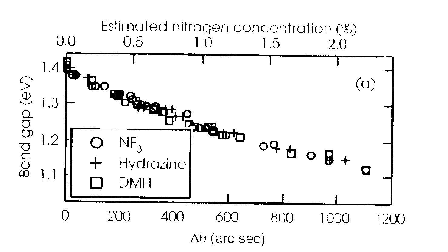
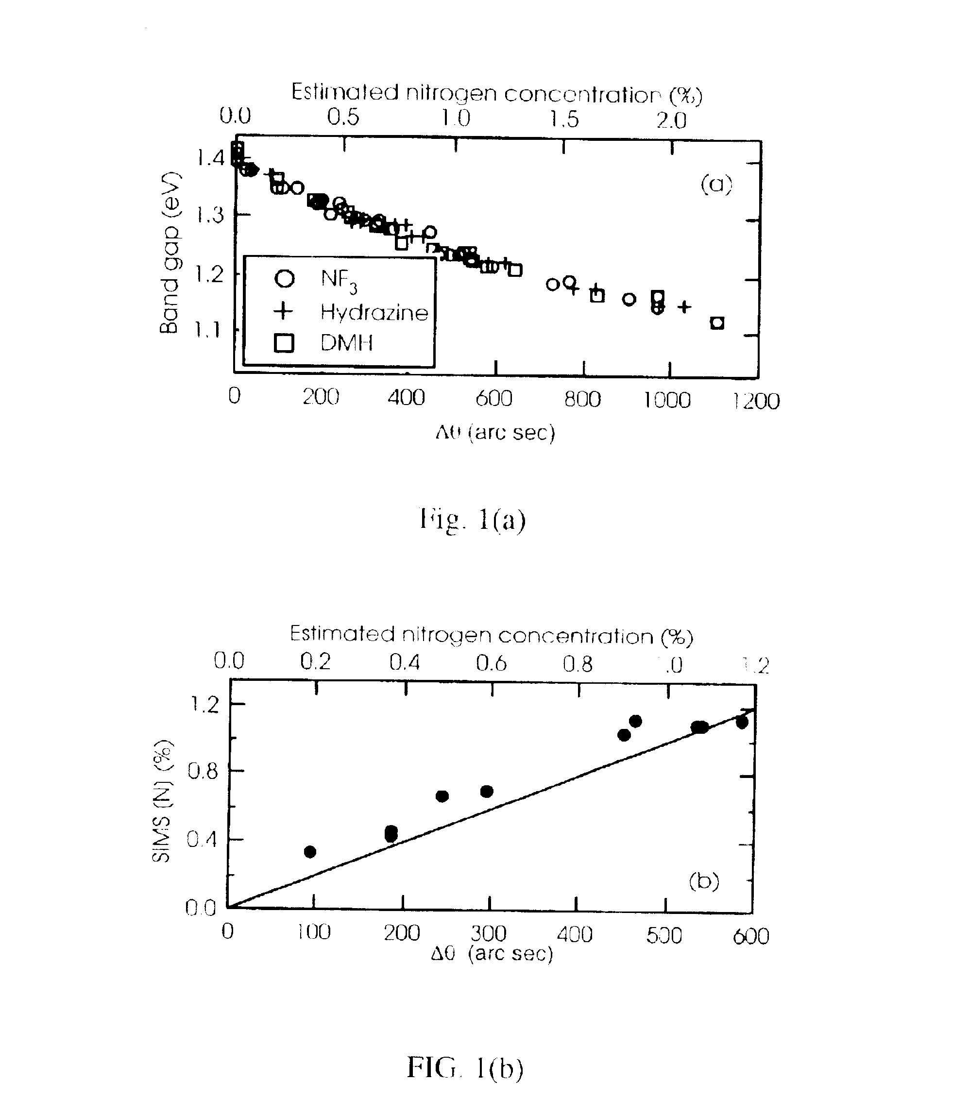
Addition of NF.sub.3 to GaAs Reduces Alloys Band Gap and Lattice Constant

Materials and Methods

The GaAsN epilayers were grown by vertical-flow, atmospheric-pressure, metal organic chemical vapor deposition (MOCVD) on GaAs substrates misoriented 2.degree. from the (100). The GaAs wafers rested on a graphite susceptor heated by radio frequency power. Arsine, timethylgallium (TMGa), triethylgallium (TEGa), u-dimethylhydrazine, and NF.sub.3 were used in a 6 slm flow of palladium-purified-hydrogen carrier. The arsine pressure was approximately 0.2 torr for the majority of the runs, although in a few runs the pressure was higher.

Note that use of hydrazine, a rocket fuel, and DMH raise serious safety issues, where the combustion of either compound is strongly exothermic. As such both compounds must be used with extreme care. NF.sub.3, on the other hand, is not a fuel, but rather an oxidizer. Oxidizers in the reducing environment provided by hydrogen mixed with arsine gas presents a potentia...

example 2

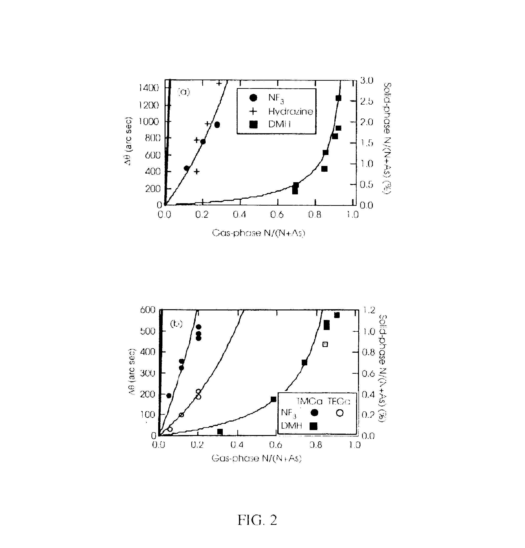
NF.sub.3 is a More Efficient Nitrogen Source Than DMH

Materials and Methods:

MOCVD nitrogen incorporation efficiency was determined by varying the N / As ratio (changing nitrogen flow), while maintaining a constant growth temperature of 550.degree. C., growth rate of 4 .mu.m / hr, and trimethylgallium as gallium source.

Results and Discussion:

Nitrogen incorporates into GaAs by MOCVD much more efficiently from NF.sub.3 than from DMH, as shown in FIG. 2. In fact, NF.sub.3 is incorporated into the GaAs with about the same efficiency as using hydrazine as the nitrogen source. Under these growth conditions, having constant arsine flow, the incorporation of nitrogen in GaAs is approximately linear with NF.sub.3 / (NF.sub.3 +As) or the concentration of DMH, respectively.

Note that the line at the left side of FIG. 2 shows the data expected if the N / As ratio in the film were the same as in the gas phase, demonstrating that the incorporation efficiency of nitrogen in GaAs by MOCVD is low, regardless ...

example 3

Nitrogen Incorporation into Gallium Arsenide is Temperature Dependent

Materials and Methods:

Epilayer growth conditions were essentially as described in Example 1. A growth rate of 4 .mu.m / hr was used for temperatures that varied from between 550.degree. C. to 700.degree. C. Nitrogen incorporation was as described in Example 1. To measure growth rate of the nitrogen incorporating alloys, all alloys were calibrated by measuring the thickness of a GaAs epilayer. This was completed using TMGa, and then again for TEGa. The TMGa and TEGa flows and the times of the growths were adjusted to grow 1 .mu.m of material, based on the calibration runs.

With regard to NF.sub.3 flow in FIG. 5, a flow of between 0.5 and 2 sccm was used and the growth rate was 2 .mu.m / hr at 550.degree. C.

Results and Discussion:

FIG. 3 illustrates the incorporation of nitrogen as a function of the growth temperature for three nitrogen precursors, NF.sub.3, hydrazine and DMH, and two gallium precursors, TMGa and TEGa. For...


PUM

PropertyMeasurementUnit
temperatureaaaaaaaaaa
pressureaaaaaaaaaa

Abstract

A method of combining group III elements with group V elements that incorporates at least nitrogen from a nitrogen halide for use in semiconductors and in particular semiconductors in photovoltaic cells.

Description

The invention relates generally to semiconductors and more particularly to the growth of nitrogen containing semiconductor material utilizing nitrogen halides as the nitrogen source.Solar energy represents a vast source of relatively non-polluting, harnessable energy. It has been estimated that the amount of solar energy striking the United States each year is over 600 times greater than all the country's energy needs. Despite this abundance, solar energy has proven difficult to economically collect, store, and transport and thus has been relatively overlooked compared to the other more conventional energy sources, i.e., oil, gas and coal. However, as conventional energy sources become less abundant and their detrimental effect on the environment continue to escalate (acid rain, air particulates, green house gasses, etc), solar energy is becoming a more viable and attractive energy source.One of the more effective ways of harnessing solar energy is through photovoltaic or solar cell...

Claims


Application Information

Patent Timeline
Patent Type & Authority Patents(United States)
IPC IPC(8): C30B25/02H01L21/205H01L21/02H01L31/18
CPCC30B25/02C30B29/40C30B29/403C30B29/406H01L21/0237H01L21/02395H01L21/02538H01L21/0254H01L21/02546H01L21/02573H01L21/0262H01L31/1844Y02E10/544
Inventor BARBER, GREG D.KURTZ, SARAH R.
Owner ALLIANCE FOR SUSTAINABLE ENERGY
Why Eureka
Try Eureka