Multiwavelength light source device employing annular optical delay circuit

a multi-wavelength light source and delay circuit technology, applied in the field of small and inexpensive multi-wavelength light source apparatuses, can solve the problems of large size of apparatuses and high cost, and achieve the effect of convenient keeping

Inactive Publication Date: 2004-09-14
ANRITSU CORP
View PDF10 Cites 10 Cited by
  • Summary
  • Abstract
  • Description
  • Claims
  • Application Information

AI Technical Summary

Benefits of technology

An object of the present invention is to provide a small-sized and inexpensive multi-wavelength light source apparatus consisting of an annular optical delay circuit which makes possible to easily keep up with an

Problems solved by technology

Therefore, in the conventional multi-wavelength light source apparatus, there are

Method used


Image

  • Multiwavelength light source device employing annular optical delay circuit
  • Multiwavelength light source device employing annular optical delay circuit
  • Multiwavelength light source device employing annular optical delay circuit

Examples


first embodiment

(First Embodiment)

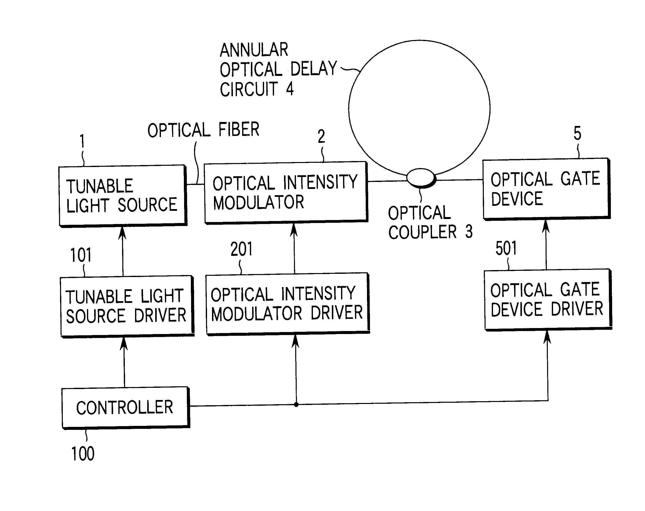
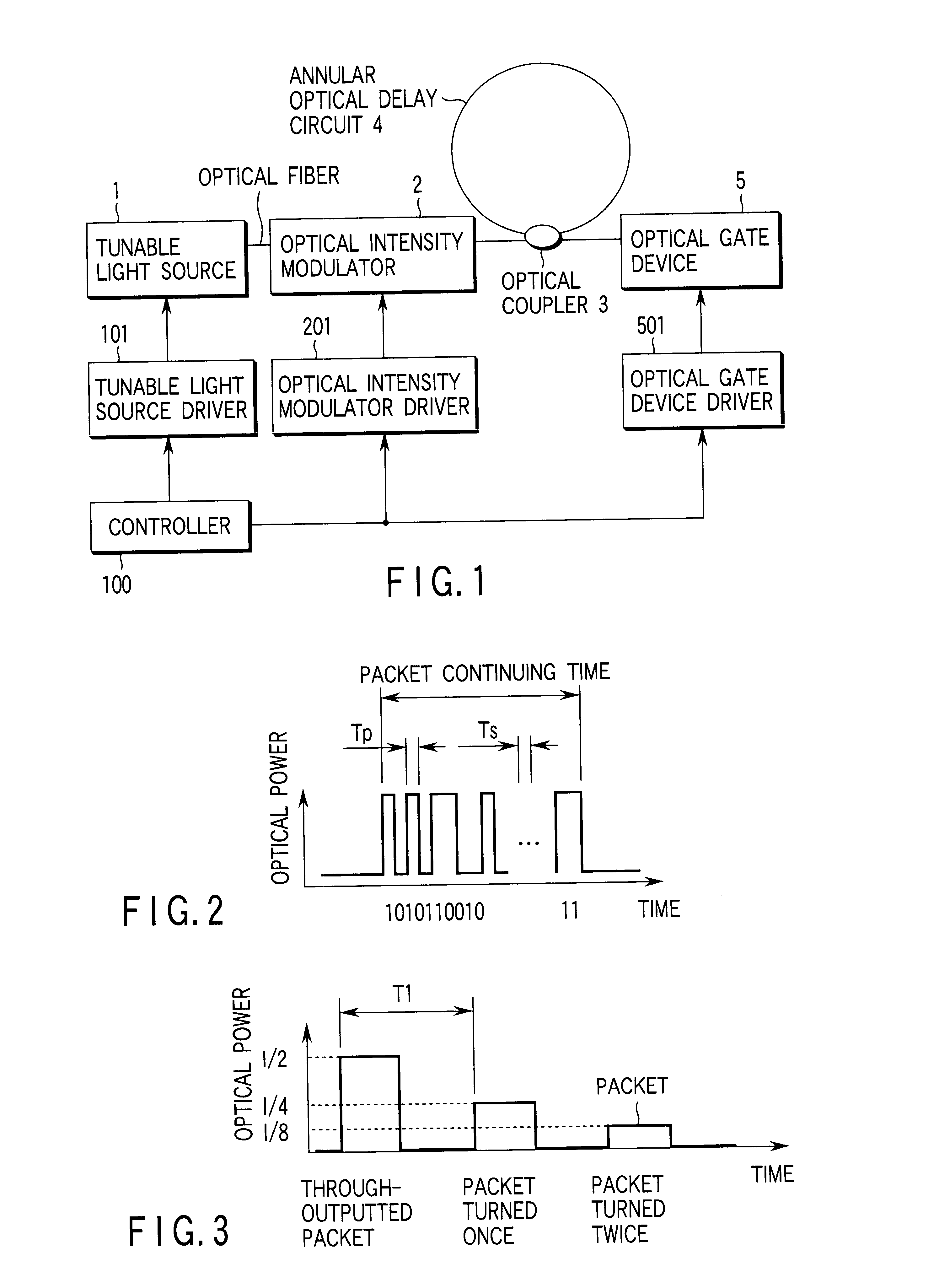
FIG. 1 is a block diagram showing a constitution of a first embodiment of the multi-wavelength light source apparatus according to the present invention.

That is, the multi-wavelength light source apparatus according to the first embodiment includes: a tunable light source 1 for successively changing and outputting a plurality of output lights different in wavelength from one another; an optical intensity modulator 2 for outputting the output light outputted from the tunable light source 1 as a modulated signal light amplitude-modulated over a predetermined time; an optical multiplexer 3, optically connected to the optical intensity modulator, for receiving the output light from the optical intensity modulator; an annular optical delay circuit 4, optically connected to the optical coupler 3, for delaying a part of the output light from the optical intensity modulator 2 over a time longer than the predetermined time; and an optical gate device 5, optically connected ...

second embodiment

(Second Embodiment)

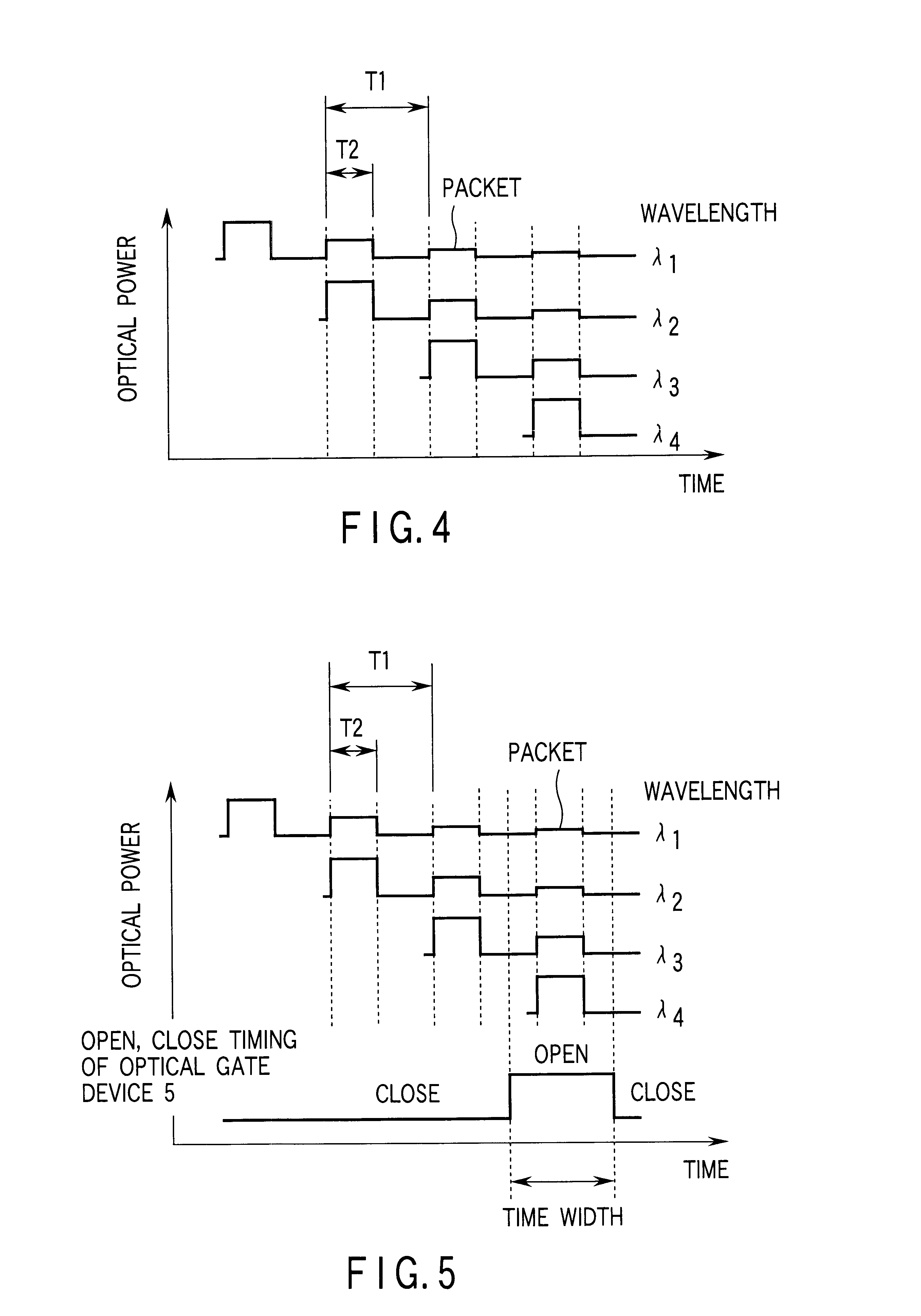
Additionally, in the constitution of the aforementioned first embodiment, the digital signal light passes the optical coupler 3 once every time the light turns around once in the annular optical delay circuit 4.

Therefore, it is assumed that the packet light intensity is set to I immediately before the packet outputted from the optical intensity modulator 2 is inputted to the optical coupler 3, and the 3 dB coupler is used as the optical coupler 3. After the light turns around N times in the annular optical delay circuit 4, the light intensity of the packet outputted to the optical gate device 5 side is represented by the following:

I.times.(1 / 2).sup.N+1.

Since the packet light intensity is attenuated by 3 dB for each turn of the packet in the annular optical delay circuit 4 in this manner, the light intensity of the digital signal light in the packet is lowered, and this gradually deteriorates a S / N ratio.

In the second embodiment, as means for solving this problem, ...

third embodiment

(Third Embodiment)

Additionally, in the optical amplifier 6 used in the second embodiment, an Amplified Spontaneous Emission (ASE) noise light is generated.

Since the ASE caused in the optical amplifier 6 is accumulated in the annular optical delay circuit 4, for the packet having a large number of turns, the S / N ratio of the digital signal light is deteriorated because of the accumulated ASE.

Therefore, in a third embodiment, as means for solving this problem, an optical frequency filter 7 is disposed together with the optical amplifier 6 in the annular optical delay circuit 4.

Here, the optical frequency filter is a filter for passing only a light having a packet optical frequency (the optical frequency of the digital signal light defined by ITU).

Since the optical frequency filter 7 is disposed together with the optical amplifier 6 in the annular optical delay circuit 4 so as to remove a frequency component other than the packet optical frequency in the ASE, the S / N ratio of the digit...


PUM


Abstract

A multi-wavelength light source apparatus includes a tunable light source, optical intensity modulator, optical coupler, annular optical delay circuit, and optical gate device. The tunable light source successively changes and outputs a plurality of output lights different in wavelength from one another. The optical intensity modulator outputs a modulated signal light obtained by modulating an amplitude of the output light outputted from the tunable light source over a predetermined time. The optical coupler is optically connected to the optical intensity modulator, and receives the light outputted from the optical intensity modulator. The annular optical delay circuit is optically connected to the optical coupler, and delays a part of the output light outputted from the optical intensity modulator over a time longer than the predetermined time. The optical gate device is optically connected to the optical coupler, receives the output light outputted from the optical intensity modulator and the light passed via the annular optical delay circuit to open a gate at a timing and time width such that all of the signal light modulated over the predetermined time is included one by one for each of the plurality of wavelengths.

Description

The present invention relates to a multi-wavelength light source apparatus, particularly to a multi-wavelength light source apparatus which outputs a digital signal light with digital information superimposed thereon and in which an annular optical delay circuit is used and makes wavelength-multiplexed packets comprising digital signal lights independent of one another simultaneously output.At present, in a field of data communication, a network mainly comprising an exchange which is "expensive" but which has guaranteed high "reliability" has been a mainstream.In near future, however, a plan for not using such exchange, and shifting to a "low-cost" next-generation data communication network utilizing an Internet apparatus has being moved forward.In the next-generation data communication network, an Internet technique is employed to divide all information such as voice represented by telephone and dynamic image into information groups called packets to be superimposed onto a digital ...

Claims


Application Information

Patent Timeline
IPC IPC(8): H04B10/155H04B10/152H04B10/50H04B10/572H04J14/02
CPCH04B10/506H04B10/572H04J14/02
Inventor KOBAYASHI, ISAOKAWAKITA, KOJIFURUKAWA, HIROSHIKINUGAWA, SHIGERU
Owner ANRITSU CORP
Why Eureka
Try Eureka