

Nonvolatile ferroelectric memory device and method of fabricating the same
a nonvolatile ferroelectric memory and nonvolatile technology, applied in semiconductor devices, digital storage, instruments, etc., can solve the problems of residual polarization, nonvolatile ferroelectric memory devices according to the related art, etc., to reduce the rate of cross-talk capacitance, reduce particle contamination, and increase production yield
- Summary
- Abstract
- Description
- Claims
- Application Information
AI Technical Summary
Benefits of technology
Problems solved by technology
Method used
Image

Examples
Embodiment Construction
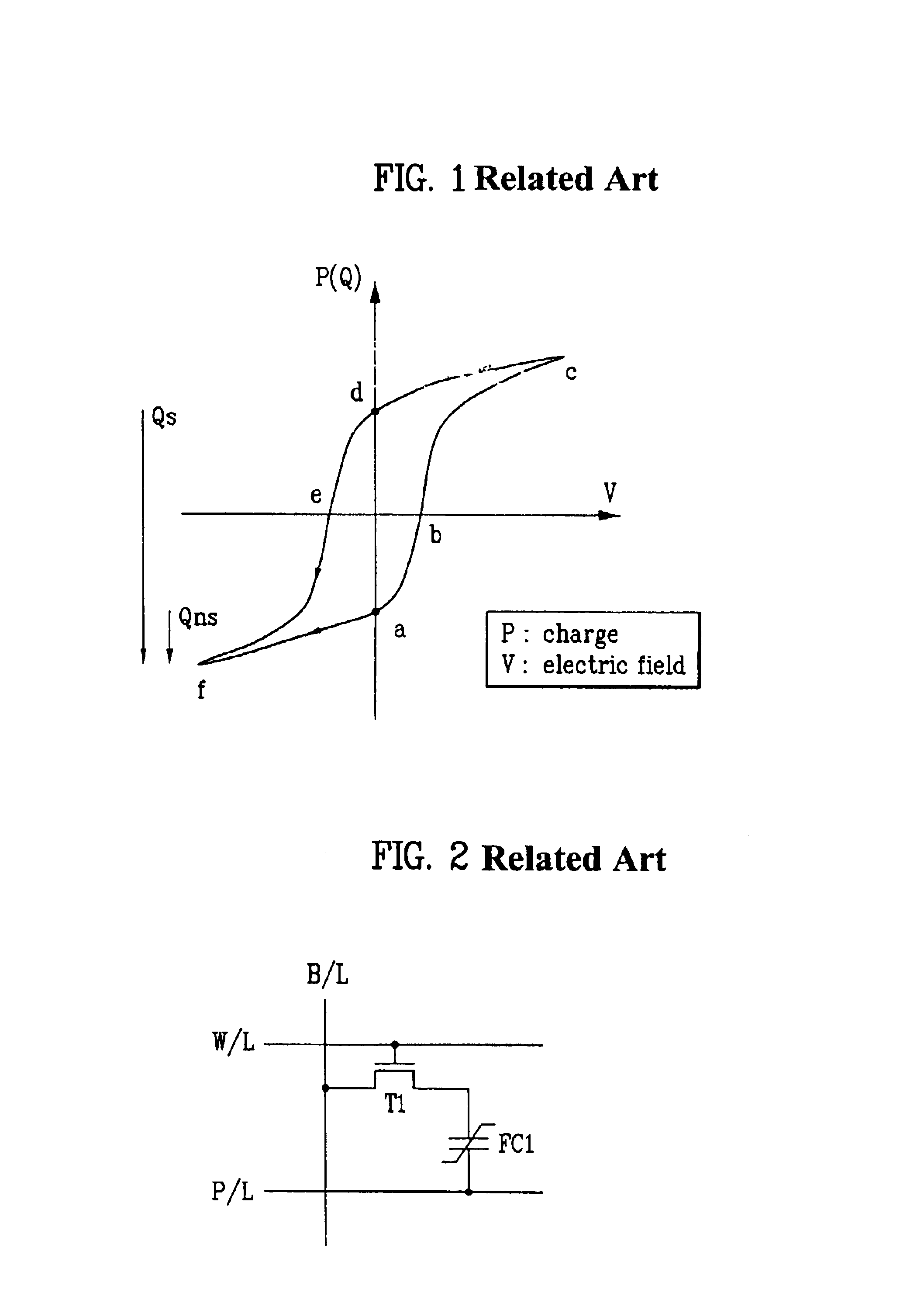
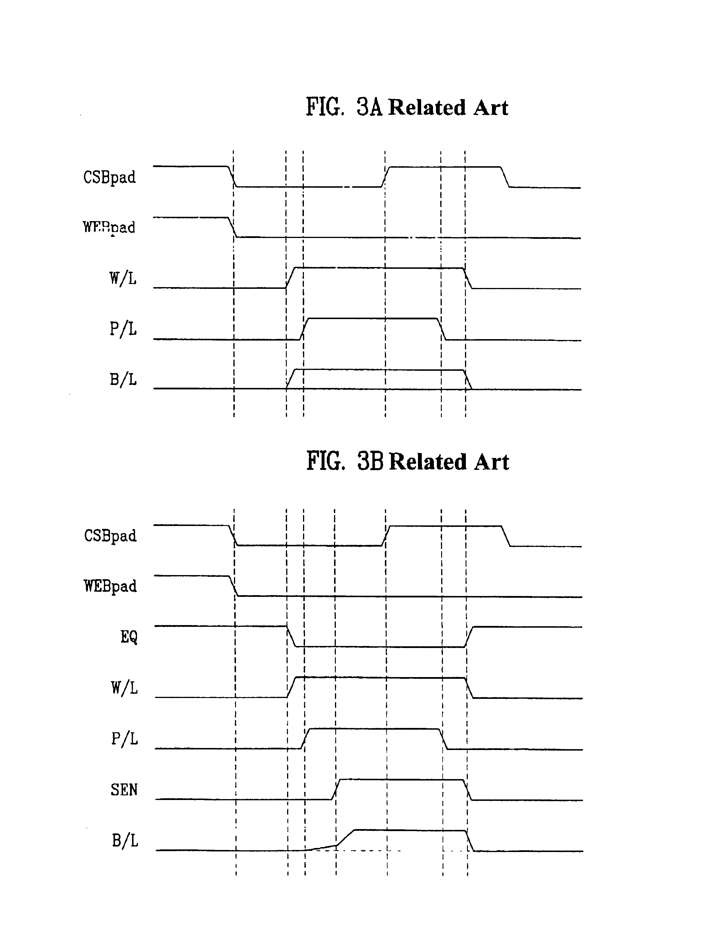
cording to the present invention;
[0033]FIG. 10 is a cross-sectional view of another exemplary metal line of a nonvolatile ferroelectric memory according to the present invention;
[0034]FIG. 11 is a cross-sectional view of another exemplary metal line of a nonvolatile ferroelectric memory according to the present invention;
[0035]FIG. 12 is a cross-sectional view of another exemplary metal line of a nonvolatile ferroelectric memory according to the present invention;
[0036]FIG. 13 is a cross-sectional view of another exemplary metal line of a nonvolatile ferroelectric memory according to the present invention; and
[0037]FIG. 14 is a cross-sectional view of another exemplary metal line of a nonvolatile ferroelectric memory according to the present invention.
DETAILED DESCRIPTION OF THE INVENTION
[0038]Reference will now be made in detail to the preferred embodiments of the present invention, examples of which are illustrated in the accompanying drawings.
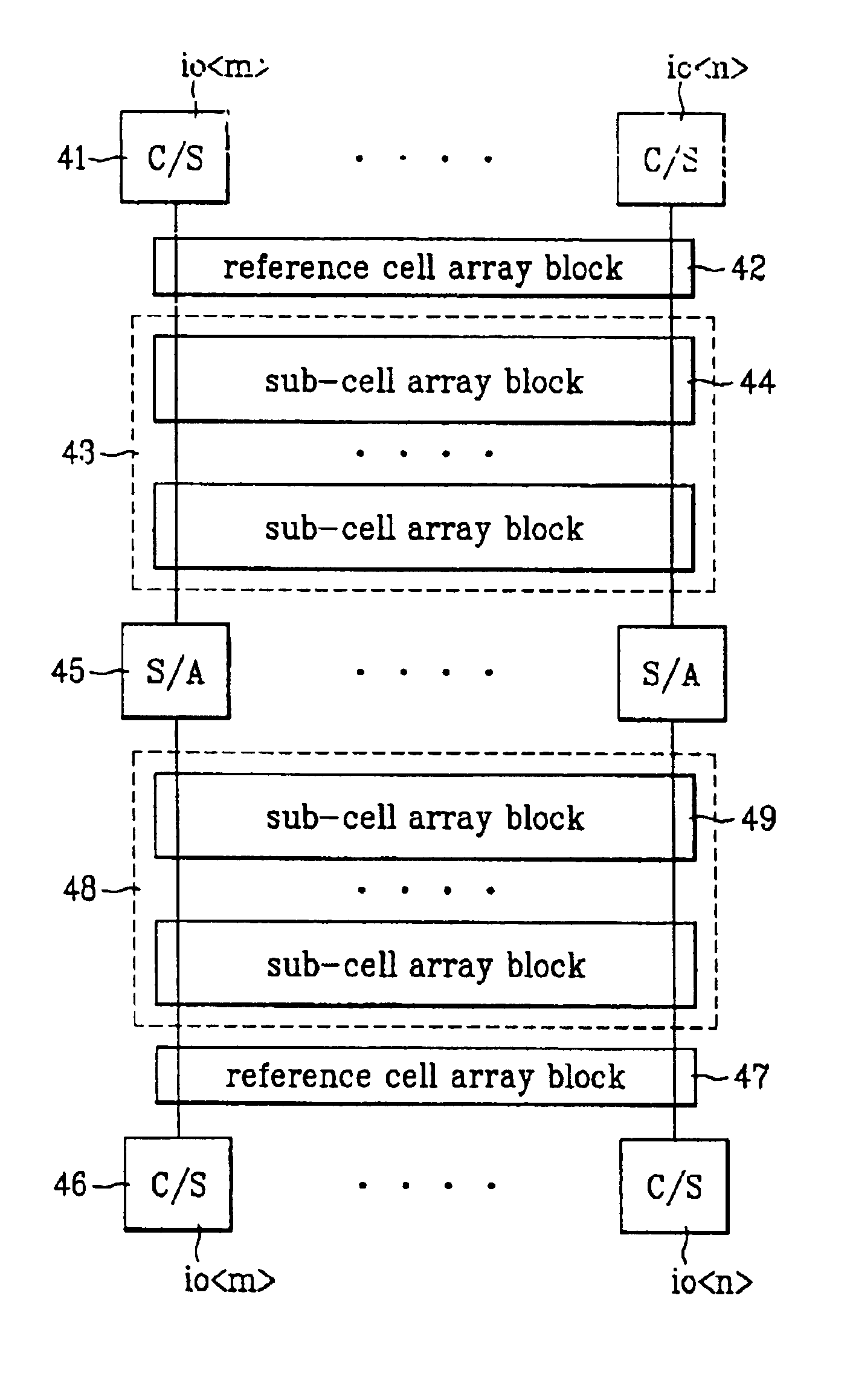
[0039]FIG. 4 is a block diagram showi...
PUM
 Abstract
Description
Claims
Application Information