Enhancement of current-carrying capacity of a multilayer circuit board

a multi-layer circuit board and current-carrying capacity technology, applied in the direction of dielectric characteristics, conductive pattern formation, printed element electric connection formation, etc., can solve the problem of inability to conformably cover the thick conductive pattern, difficulty in miniaturizing the conductive pattern, and inability to etch the conductive pattern accurately when the conductive pattern is patterned out, etc. problem, to achieve the effect of increasing the current-carrying capacity

Inactive Publication Date: 2005-02-01
MURATA MFG CO LTD
View PDF5 Cites 34 Cited by
  • Summary
  • Abstract
  • Description
  • Claims
  • Application Information

AI Technical Summary

Benefits of technology

The present invention has been made in view of the above aspects with an object to increase the current-carrying capacity of a multilayer circuit board without thickening a conductive pattern included in the board.

Problems solved by technology

However, if the current-carrying capacity was increased by thickening the conductive patterns, it would become difficult to miniaturizing the conductive patterns because the etching precision when the conductive patterns are patterned out by etching would worsen.
Moreover, if extremely thick conductive patterns were used, the thermoplastic resin films, on which the thick conductive patterns have been formed, could not conformably cover the thick conductive patterns when the thermoplastic resin films are molten by heat pressed.

Method used


Image

  • Enhancement of current-carrying capacity of a multilayer circuit board
  • Enhancement of current-carrying capacity of a multilayer circuit board
  • Enhancement of current-carrying capacity of a multilayer circuit board

Examples


first embodiment

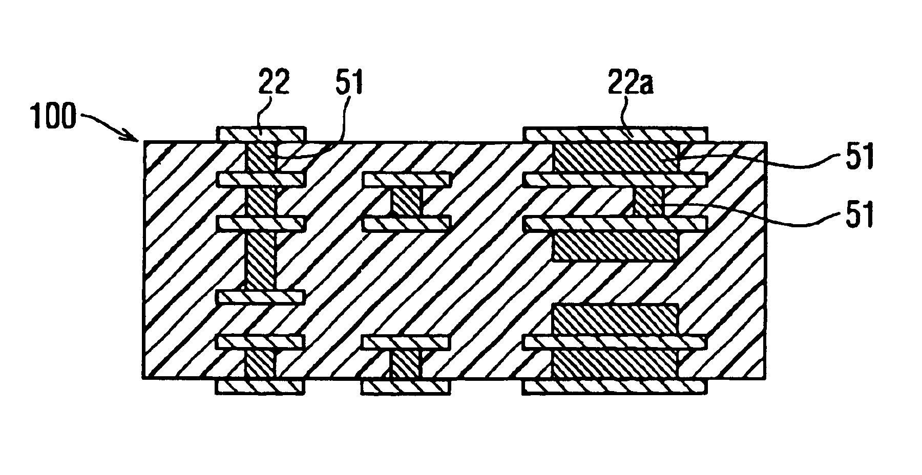
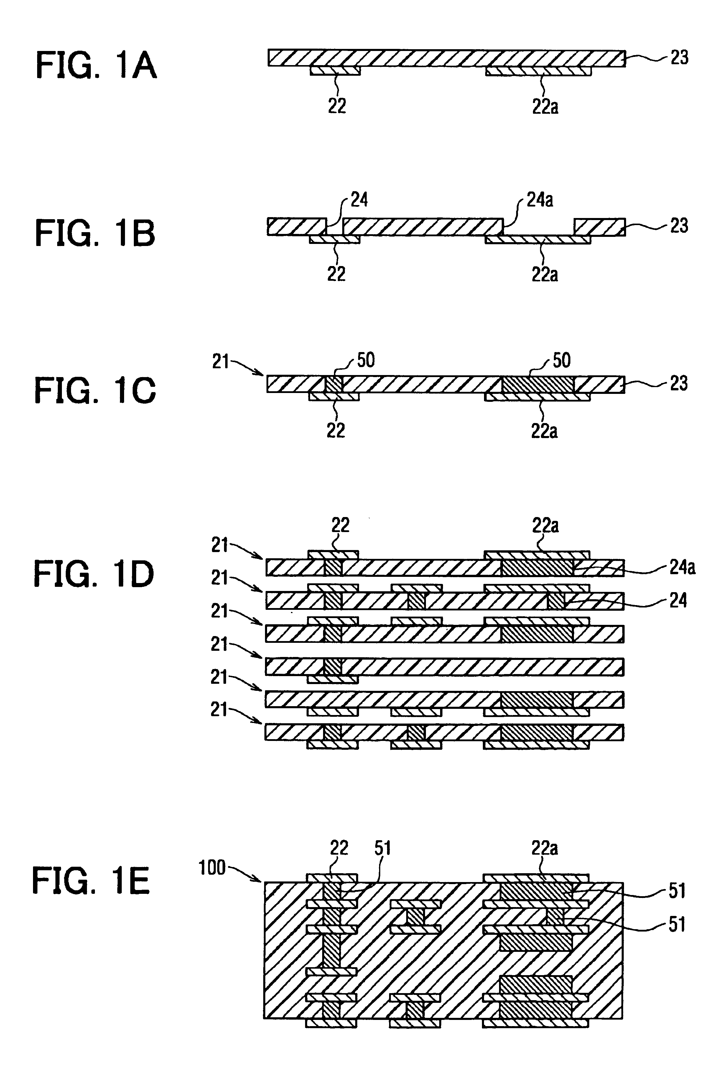
A multilayer circuit board 100 of FIG. 1E according to the first embodiment is manufactured using the steps shown in FIGS. 1A to 1E. First, a single-sided conductive pattern film 21 of FIG. 1C is formed using the steps shown in FIGS. 1A to 1C. First, a copper foil having a thickness of 18 μm and a thermoplastic resin film 23, which becomes an insulating layer in the multilayer circuit board 100 of FIG. 1E, are laminated, and then the copper foil is patterned into a first conductive pattern 22 and a second conductive pattern 22a by etching, as shown in FIG. 1A.

The conductive pattern 22, 22a are made of copper and have a thickness of 18 μm. However, the conductive pattern 22, 22a may be made of other metal. In addition, the thickness may not be 18 μm. However, the thickness is preferably in the range from 5 to 75 μm in consideration of the etching precision when the conductive pattern 22, 22a are formed by etching and the voids that would otherwise be generated when a plurality of sin...


PUM

PropertyMeasurementUnit
thicknessaaaaaaaaaa
thicknessaaaaaaaaaa
thicknessaaaaaaaaaa

Abstract

A multilayer circuit board, in which a plurality of insulating layers and a plurality of conductive layers, each of which includes a conductive pattern, have been laminated, includes an insulating layer, a conductive compound, and a conductive pattern. The insulating layer has a trench. The conductive compound is located in the trench. The conductive pattern adjoins the trench and is electrically connected to the conductive compound. The conductive pattern and the conductive compound make up a conductive wire that has a higher current-carrying capacity than the conductive pattern.

Description

CROSS REFERENCE TO RELATED APPLICATIONThis application is based on and incorporates herein by reference Japanese Patent Application No. 2002-158041 filed on May 30, 2002.BACKGROUND OF THE INVENTIONThe present invention relates to a multilayer circuit board electrified with a high current and a method for manufacturing the multilayer circuit board.Multilayer circuit boards have been lately in great demand for densely packaging semiconductor devices and electric components such as a condenser and a resistor. Such a multilayer circuit board can be manufactured, for example, by: stacking conductive pattern films, in each of which conductive patterns made of, for example, copper have been patterned out on a thermoplastic resin film, which is an insulating layer; and integrating the stacked body by heat pressing.With respect to the above multilayer circuit board, there have been demands, for example, for mounting a power device on the board in order to form a power source circuit or for b...

Claims


Application Information

Patent Timeline
Patent Type & Authority Patents(United States)
IPC IPC(8): H01L23/498H01L23/48H05K3/46H05K3/40H05K1/02H01L23/12H05K3/10H05K3/24
CPCH01L23/498H01L23/49822H01L23/49838H05K3/4617H05K3/4632H05K3/4069Y10T29/49165H05K2201/0394H05K2201/09881H01L2924/0002H05K2201/0129H01L2924/00H05K3/46
Inventor KONDO, KOJIKATAOKA, RYOHEIMASUDA, GENTARO
Owner MURATA MFG CO LTD
Why Eureka
Try Eureka