Microfluidic devices having a reduced number of input and output connections

a technology of microfluidic devices and input/output connections, applied in flow control, fluid speed measurement, sampled variable control systems, etc., can solve the problem that multi-component devices can be easily assembled into complex, integrated systems, and achieve the effect of reducing the number of input/output connections

Inactive Publication Date: 2005-02-08
HANDYLAB
View PDF153 Cites 227 Cited by
  • Summary
  • Abstract
  • Description
  • Claims
  • Application Information

AI Technical Summary

Benefits of technology

The invention relates generally to techniques for reducing the number of input / output connections required to connect a microfluidic substrate to an external controller for controlling the substrate. In one aspect, the invention involves a microfluidic processing device fabricated on a substrate having a plurality of N independently controllable components, (e.g., resistive heating elements) each having at least two terminals. The substrate includes a plurality of input / output contacts for connecting the substrate to an external controller, and a plurality of leads for connecting the contacts to the terminals of the components. The leads are arranged to allow the external controller to supply control signals to the terminals of the components via the contacts using substantially fewer contacts than the total number of component terminals. For example, in one embodiment, each lead connects a corresponding contact to a plurality of terminals to allow the controller to supply to signals to the terminals without requiring a separate contact for each terminal. However, to assure that the components can each be controlled independently of the others, the leads are also arranged so that each component's terminals are connected to a unique combination of contacts. Thus, the external controller can activate a selected component by supplying control signals to the combination of contacts uniquely associated with that component.

Problems solved by technology

Because all of the components are made using conventional photolithographic techniques, multi-component devices can be readily assembled into complex, integrated systems.

Method used


Image

  • Microfluidic devices having a reduced number of input and output connections
  • Microfluidic devices having a reduced number of input and output connections
  • Microfluidic devices having a reduced number of input and output connections

Examples


Embodiment Construction

System Overview

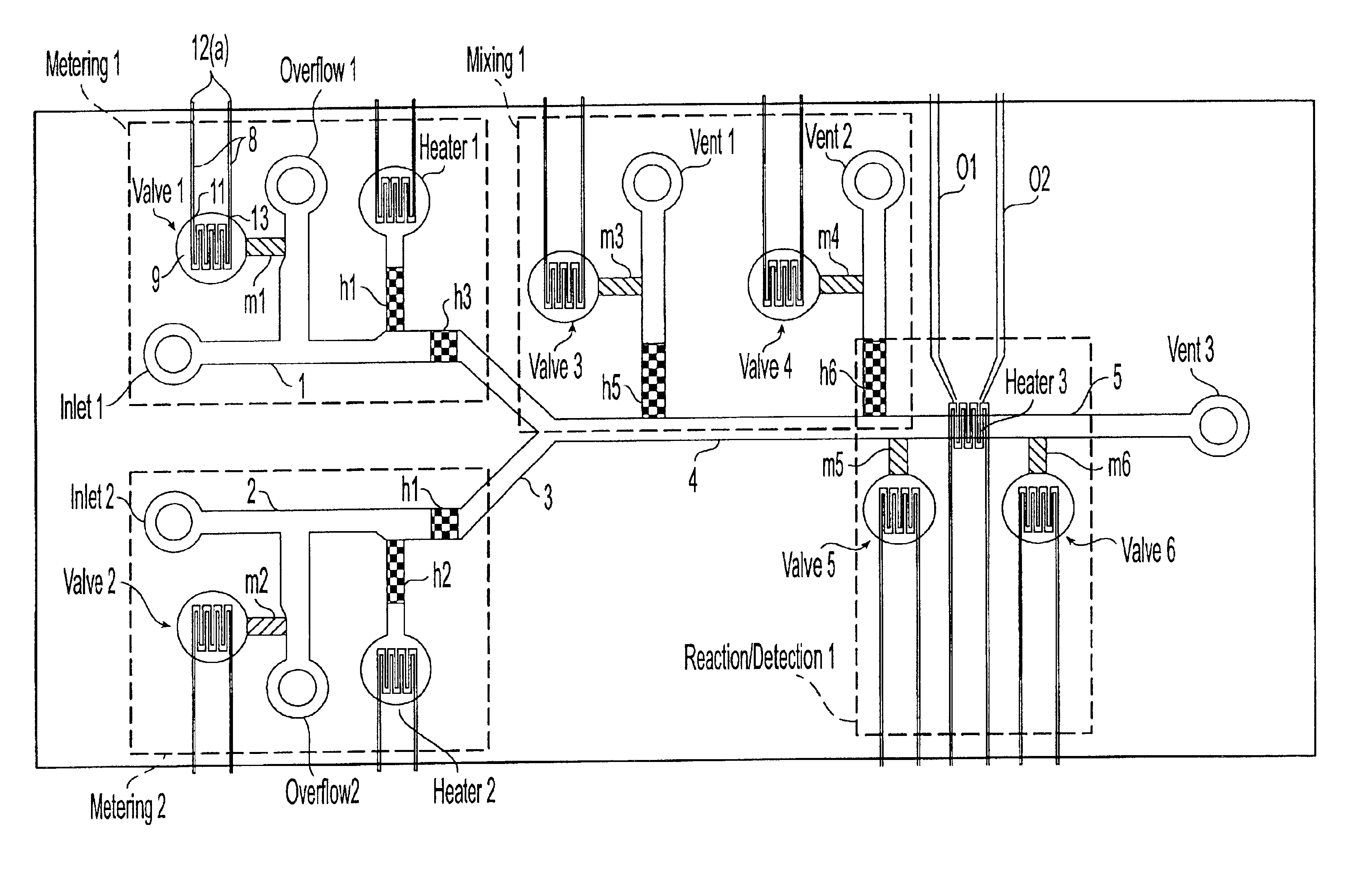
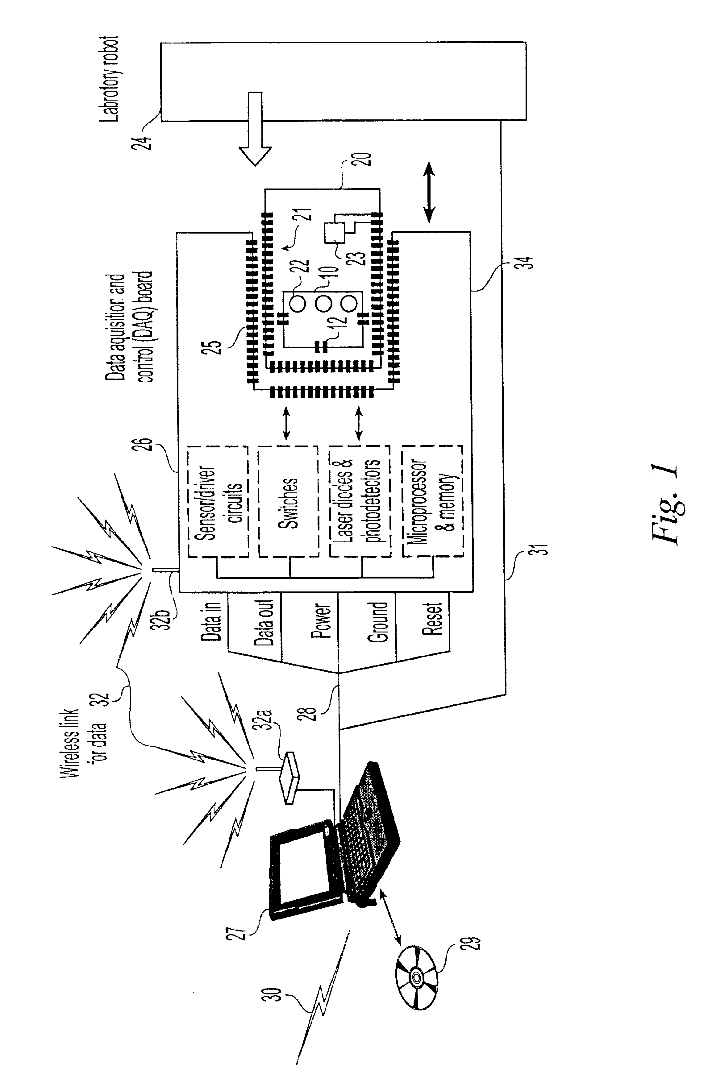
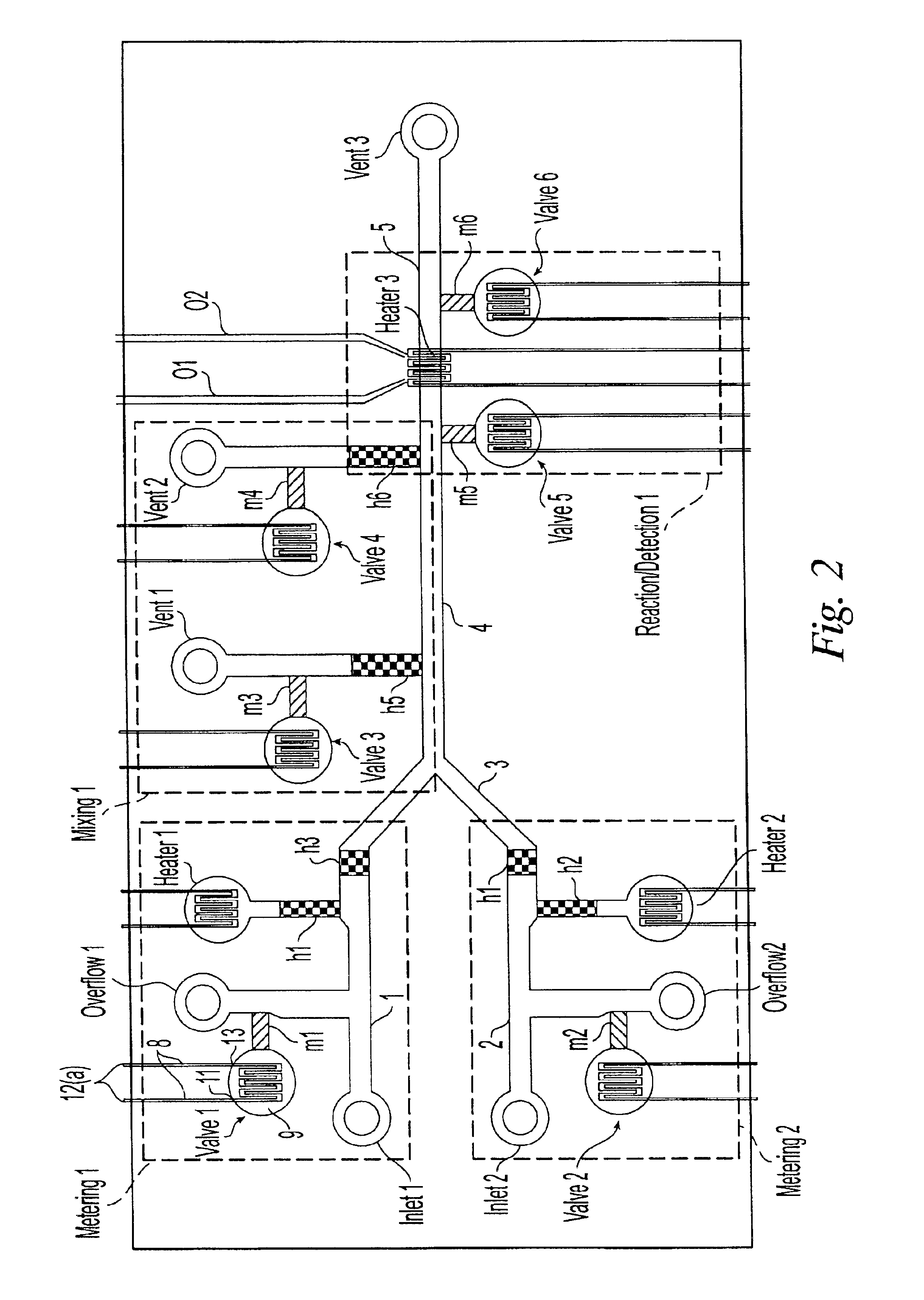
FIG. 1 depicts a microfluidic processing system that includes a microfluidic substrate 10, a chip carrier cartridge 20, a data acquisition and control board (“DAQ”) 26, and a portable computer 27 such as a laptop or palmtop computer. Microfluidic substrate 10 has microchannels and fluid control elements formed in a solid substrate such as silicon, glass, or other suitable material, preferably microfabricated using conventional photolithographic techniques. The microfluidic substrate 10 is mounted on the chip carrier cartridge 20. The microfluidic substrate 10 has electrical and optical connections 12 with the chip carrier cartridge for carrying electrical and optical signals between the microfluidic substrate and the chip carrier. For example, the electrical connections can be formed with well-known wire bonding techniques. Furthermore, the chip carrier cartridge 20 has electrical and optical contacts 21 for carrying electrical and optical signals between the microflu...


PUM

PropertyMeasurementUnit
output voltageaaaaaaaaaa
chemicalaaaaaaaaaa
electrophoretic forcesaaaaaaaaaa

Abstract

A system and method for reducing the number of input/output connections required to connect a microfluidic substrate to an external controller for controlling the substrate. In one example, a microfluidic processing device is fabricated on a substrate having a plurality of N independently controllable components, (e.g., a resistive heating elements) each having at least two terminals. The substrate includes a plurality of input/output contacts for connecting the substrate to an external controller, and a plurality of leads for connecting the contacts to the terminals of the components. The leads are arranged to allow the external controller to supply control signals to the terminals of the components via the contacts using substantially fewer contacts than the total number of component terminals. For example, in one embodiment, each lead connects a corresponding contact to a plurality of terminals to allow the controller to supply to signals to the terminals without requiring a separate contact for each terminal. However, to assure that the components can each be controlled independently of the others, the leads are also arranged so that each component's terminals are connected to a unique combination of contacts. Thus, the external controller can activate a selected component by supplying control signals to the combination of contacts uniquely associated with that component.

Description

FIELD OF THE INVENTIONThe present invention relates to microfluidic devices, and more particularly to techniques for reducing the number of input and output connections required to connect a microfluidic device to an external controller for controlling the microfluidic device.BACKGROUND OF THE INVENTIONMicro / nano technology devices are known in the art as devices with components on the scale of 1 μm to 100s of μm that cooperate to perform various desired functions. In particular, microfluidic devices are micro / nano technology devices that perform fluid handling functions which, for example, cooperate to carry out a chemical or biochemical reaction or analysis.Microfluidic devices include a variety of components for manipulating and analyzing the fluid within the devices. Typically, these elements are microfabricated from substrates made of silicon, glass, ceramic, plastic, and / or quartz. These various fluid-processing components are linked by microchannels, etched into the same subs...

Claims


Application Information

Patent Timeline
Patent Type & Authority Patents(United States)
IPC IPC(8): B01L3/00G01N35/00B01J19/00B81B1/00G01N37/00
CPCB01L3/502715B01L7/00B01L3/502746G05D7/0617Y10T436/12B01L3/502738B01L2200/02B01L2200/14B01L2200/147B01L2300/02B01L2300/0819B01L2300/1827B01L2400/0442B01L2400/0677Y10T436/2575B01L3/50273Y10T137/0318
Inventor GANESAN, KARTHIK
Owner HANDYLAB
Why Eureka
Try Eureka