Semiconductor memory enabling correct substitution of redundant cell array
Active Publication Date: 2005-02-08
INFINEON TECH LLC
View PDF2 Cites 44 Cited by
- Summary
- Abstract
- Description
- Claims
- Application Information
AI Technical Summary
Benefits of technology
[0015]Accordingly, in a semiconductor memory which substitutes a redundant cell array for an area including a defective cell, it is an object of the present invention to provide the semiconductor memory capable of correctly substituting the redundant cell array irrespective of the defective cell location.
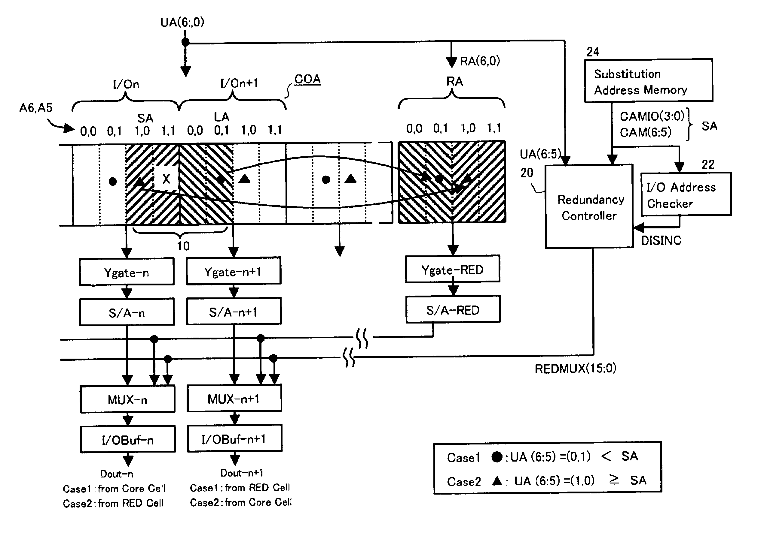
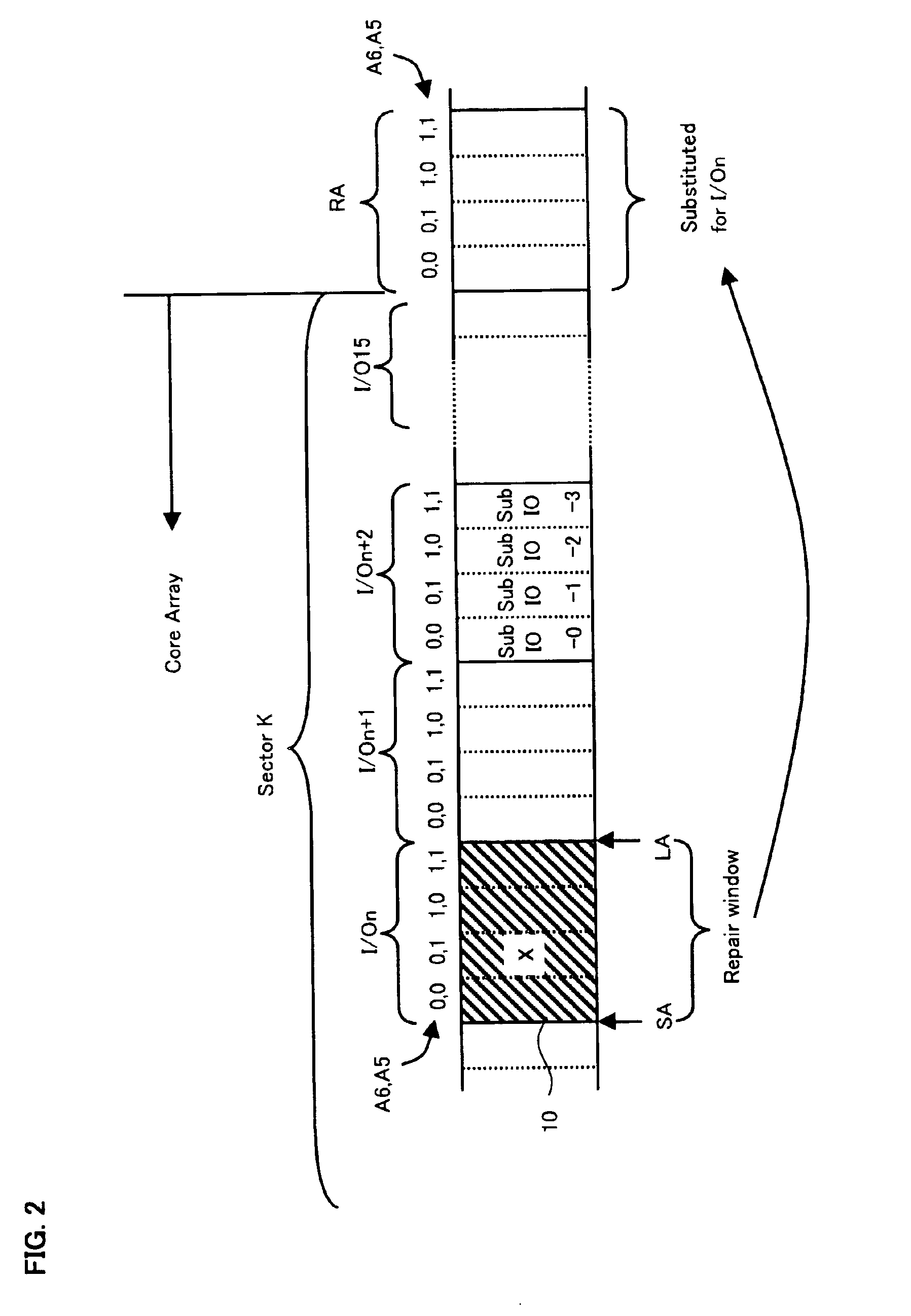
[0017]According to the above-mentioned first aspect of the present invention, in the memory test process, the address of the first substitution object area which includes both sides of the detected defective cell is stored in the substitution address memory. When the defective cell is located in the edge portion of the core array, there arises an inconvenience that a portion of the first substitution object area is located on the outside of the core array. To avoid this inconvenience, the redundancy controller automatically controls to substitute the redundant array for a second substitution object area which includes the defective cell but does not include the outside area of the core array, in place of the first substitution object area. Thus, it becomes possible in the test process to obtain the substitution object address to be stored in the substitution address memory uniformly by use of an identical logic operation, irrespective of the defective cell location. Thus, a simplified test process as well as a reduced production cost can be attained. The redundancy controller can eliminate the aforementioned inconvenience produced in the test process.
Problems solved by technology
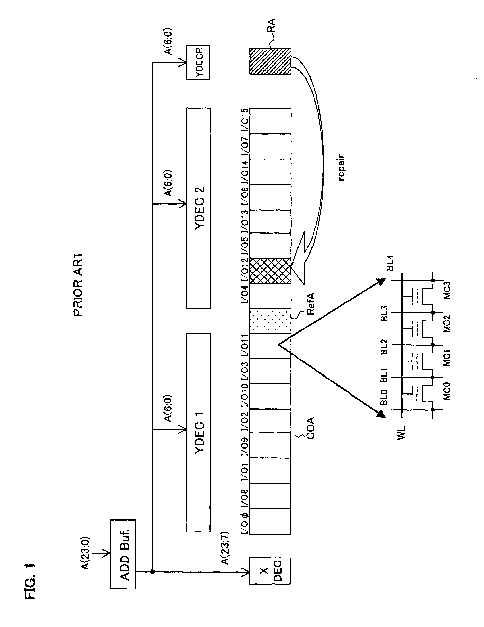
When the defective cell is located in the edge portion of the core array, there arises an inconvenience that a portion of the first substitution object area is located on the outside of the core array.
Method used
View moreImage
Smart ImageViewing Examples
Examples
first embodiment
[0031]FIG. 9 shows a logic circuit diagram of an I / O address checker in accordance with the present invention.
second embodiment
[0032]FIG. 10 shows a configuration diagram of the semiconductor memory in accordance with the present invention.
[0033]FIG. 11 shows a configuration diagram of the semiconductor memory in accordance with the second embodiment of the present invention.
[0034]FIG. 12 shows a configuration diagram of the semiconductor memory in accordance with the second embodiment of the present invention.
[0035]FIG. 13 shows a logic circuit diagram of an I / O page address checker in accordance with the second embodiment of the present invention.
Login to View More PUM
 Abstract
A semiconductor memory includes a core array including a plurality of memory cells, and a redundant array to be substituted for a substitution object area having a defective cell in the core array. In this semiconductor memory, there are provided a substitution address memory which stores an address of a first substitution object area including both sides of the defective cell as a substitution object address, and a redundancy controller which controls to substitute the redundant array for the substitution object area of the core array. When a portion of the first substitution object area is located on the outside of the core array, the redundancy controller controls to substitute the redundant array for a second substitution object area which has the defective cell and is located on the inside of the core array.
Description
CROSS-REFERENCE TO RELATED APPLICATIONS[0002]This application is based upon and claims the benefit of priority from the prior Japanese Patent Application No. 2002-267680, filed on Sep. 13, 2002, the entire contents of which are incorporated herein by reference.FIELD OF THE INVENTION[0003]The present invention relates to a semiconductor memory having a redundant cell array and more particularly a semiconductor memory in which the redundant cell array is correctly substituted for a defective cell area in a core array.BACKGROUND OF THE INVENTION[0004]As the semiconductor memory has become larger in scale with micro-fabrication technology, a defective cell may exist in a core array with an increased possibility. A defect in the memory cell itself may cause such a defective cell, as well as a short circuit between neighboring bit lines may constitute one of other major causes. Such a defective cell is normally detected in the test process before the shipment, and the detected defective c...
Claims
Login to View More Application Information
Patent Timeline
 IPC IPC(8): G11C29/00G11C16/06G11C29/04
CPCG11C29/846G11C29/808G11C29/00
Inventor CHEUNG, ANDY
Owner INFINEON TECH LLC


