Reduce 1/f noise in NPN transistors without degrading the properties of PNP transistors in integrated circuit technologies

a technology of integrated circuit technology and transistors, which is applied in the direction of transistors, electrical equipment, semiconductor devices, etc., can solve the problems of 1/f noise, 1/f noise, and high 1/f noise, and achieve the effect of reducing the 1/f noise in the transistor

Inactive Publication Date: 2005-02-15
TEXAS INSTR INC
View PDF2 Cites 6 Cited by
  • Summary
  • Abstract
  • Description
  • Claims
  • Application Information

AI Technical Summary

Benefits of technology

The instant invention describes a method for reducing the 1 / f noise in NPN bipolar junction transistors. In particular a collector region is formed in a semiconductor substrate. A base region is formed in the collector region. A partial emitter region is formed in the base region. In an embodiment of the instant invention the collector is n-type and is formed by growing an n-type epitaxial layer. A p-type base region is formed in the collector region by implanting p-type dopants into the collector region. For an n-type partial emitter region, n-type dopants are implanted into the base region. An interfacial oxide layer is then formed on the partial emitter region and a polysilicon layer is formed on the interfacial oxide layer. For an n-type emitter region, n-type dopants are implanted into the polysilicon region over the partial emitter region to complete the emitter region formation. In addition to the n-type dopants, a fluorine containing species is implanted into the polysilicon region to reduce the 1 / f noise in the transistor. The fluorine containing species is selectively introduced into the NPN transistor and not in the PNP transistor.

Problems solved by technology

Increasing IFO thickness in NPN transistors was found to dramatically increase the low frequency output noise of the transistor (i.e., 1 / f noise).
High 1 / f noise can have a detrimental effect on the use of NPN transistors in integrated circuit applications such as in the input stage of high performance operational amplifiers.

Method used


Image

  • Reduce 1/f noise in NPN transistors without degrading the properties of PNP transistors in integrated circuit technologies
  • Reduce 1/f noise in NPN transistors without degrading the properties of PNP transistors in integrated circuit technologies
  • Reduce 1/f noise in NPN transistors without degrading the properties of PNP transistors in integrated circuit technologies

Examples


Embodiment Construction

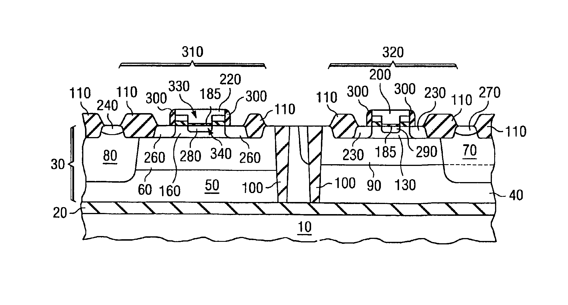
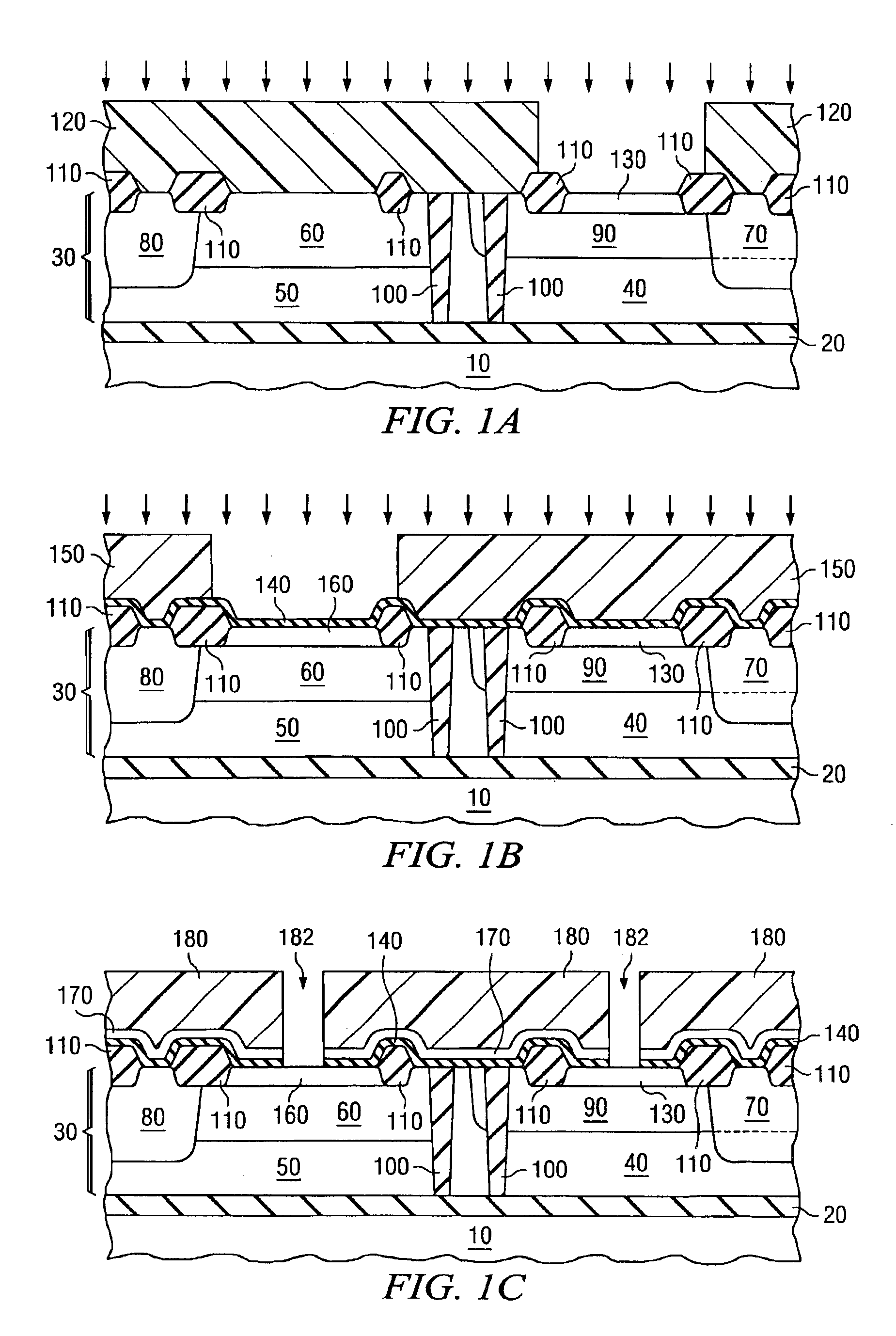
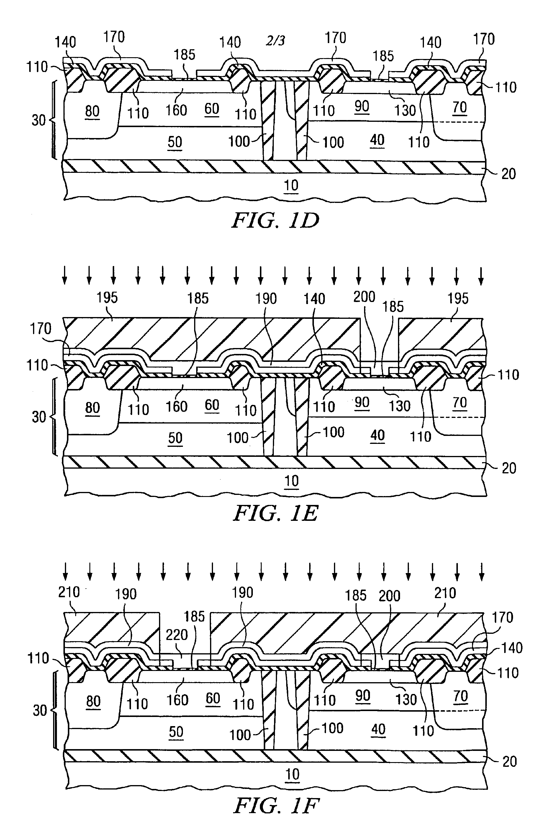
The instant invention comprises forming a fluorinated IFO in a poly-emitter bipolar junction transistor (BJT). The fluorinated IFO reduces the 1 / f noise in NPN transistors without affecting the HFE or Va of the PNP transistor. The method of fluorinated IFO formation comprises introducing a fluorine containing species into the polysilicon emitter of the NPN BJT during formation. The method will be described with reference to an integrated circuit process for forming PNP and NPN transistors. It should however be noted that the method applies to the formation of a fluorinated IFO and can be used in any semiconductor device requiring an IFO.

Shown in FIGS. 1(a)-1(i) are cross-sectional diagrams showing an embodiment of the instant invention. Shown in FIG. 1(a) is a semiconductor substrate after a number of processing steps. As shown in FIG. 1(a), silicon on insulator (SOI) substrates are used in the illustrated embodiment. Silicon on insulator substrates usually comprise a first silicon ...


PUM


Abstract

An interfacial oxide layer (185) is formed in the emitter regions of the NPN transistor (280, 220) and the PNP transistor (290, 200). Fluorine is selectively introduced into the polysilicon emitter region of the NPN transistor (220) to reduce the 1/f noise in the NPN transistor.

Description

FIELD OF THE INVENTIONThe present invention relates to a method to reduce the 1 / f noise in NPN transistors without degrading the properties in PNP transistors in integrated circuits containing both NPN and PNP transistors.BACKGROUND OF THE INVENTIONThe electrical properties of polycrystalline silicon emitter (poly-emitter) bipolar junction transistors (BJT) are strongly influenced by the properties of the interfacial oxide (IFO) that exists between the polycrystalline silicon (polysilicon) emitter and the crystalline emitter. For example, the current gain (HFE) of the BJT can be enhanced by a thicker IFO layer. The current gain HFE is defined as the ratio of the corresponding change in transistor collector current δIc to a change in the transistor base current δIB. In addition to a higher HFE, an accompanying increase in the Early Voltage (Va) is obtained in PNP transistors for thicker IFO layers. The increase in HFE and accompanying increase in Va are very desirable properties of P...

Claims


Application Information

Patent Timeline
Patent Type & Authority Patents(United States)
IPC IPC(8): H01L21/70H01L21/331H01L21/02H01L29/08H01L29/02H01L21/8228H01L27/082
CPCH01L21/82285H01L29/66287H01L29/0804H01L27/0826
Inventor TROGOLO, JOE R.LOFTIN, WILLIAMKYSER, JR., WILLIAM F.
Owner TEXAS INSTR INC
Why Eureka
Try Eureka