Reduced 1/f noise in MOSFETs

a technology of mosfet and mosfet, which is applied in the direction of semiconductor devices, semiconductor device details, electrical apparatus, etc., can solve the problems of nitride oxides introducing undesirable side effects, boron penetration is generally only a problem, and the device performance is affected.

Inactive Publication Date: 2003-11-25
NEWPORT FAB
View PDF19 Cites 5 Cited by
  • Summary
  • Abstract
  • Description
  • Claims
  • Application Information

AI Technical Summary

Benefits of technology

The present invention relates to reducing the 1 / f noise in MOSFET devices. One embodiment of the present invention is a gate for a MOSFET device located on a semiconductor substrate. The gate includes a thin gate oxide layer formed on the semiconductor substrate. Nitrogen is selectively implanted into the semiconductor substrate at a location proximate to the thin gate oxide layer. The gate also includes a gate electrode in contact with the thin gate oxide layer.

Problems solved by technology

Changes in the boron penetration produce fluctuations in the threshold voltage which impact the performance of the device.
In a dual gate thickness CMOS process technology, where thin and thick gate oxides for MOSFET devices are formed, boron penetration is generally only a problem for thin gate oxide MOSFETs.
Unfortunately, nitrided oxides introduce some undesirable side effects.
The use of nitrided oxides significantly increases the 1 / f noise or "flicker noise" in MOSFETs through an introduction of oxide charges and traps.
These levels of 1 / f noise are particularly unattractive for analog / RF circuit applications due to the impact upon key circuit metrics such as noise figure and oscillator phase noise.
However, VHP nitridation requires the use of a very high pressurized reacting chamber that is very expensive to utilize in a manufacturing process.
Further, VHP nitridation is hard to implement because of safety reasons.

Method used


Image

  • Reduced 1/f noise in MOSFETs
  • Reduced 1/f noise in MOSFETs
  • Reduced 1/f noise in MOSFETs

Examples


Embodiment Construction

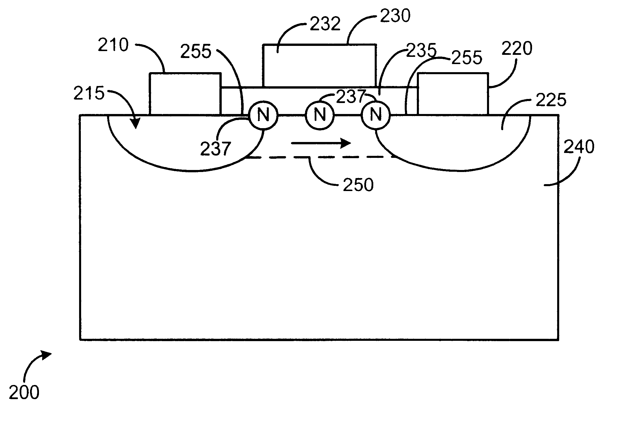
The present invention may be described herein in terms of various hardware components and processing steps. It should be appreciated that such components may be realized by any number of hardware components configured to perform the specified functions. For example, the present invention may employ various integrated circuit components, e.g., transistors, memory elements, digital signal processing elements, integrators, and the like, which may carry out a variety of functions under the control of one or more microprocessors or other control devices. In addition, those skilled in the art will appreciate that the present invention may be practiced in any number of field effect transistor contexts and that the preferred embodiment described herein is merely one exemplary application for the invention. Accordingly, the present invention is not limited to the process flows described herein, as any process flow or rearrangement of process steps which captures the features of the present i...


PUM


Abstract

An improved gate structure for a MOSFET device exhibits a reduced level of 1 / f noise or "flicker noise", while maintaining the control of boron penetration into the substrate of the MOSFET device. The gate structure for the MOSFET device includes a gate electrode and a gate oxide layer wherein nitrogen is selectively implanted into the gate oxide / device substrate interface prior to oxidation of the gate oxide layer. The nitrogen is selectively implanted so that the nitrogen is implanted into thin gate oxide regions and masked from thick gate oxide regions so that the benefits of controlling the boron penetration are realized while the 1 / f noise is reduced due to the selective implantation of the nitrogen.

Description

BACKGROUND OF THE INVENTION1. Technical FieldThe present invention relates generally to microelectronic circuits. More specifically, the present invention relates to reducing 1 / f noise in Metal Oxide Semiconductor Field Effect Transistor (MOSFET) devices.2. Background InformationNitrided oxides are commonly used as gate dielectrics in submicron Complementary Metal-Oxide Semiconductor (CMOS) technologies due to the nitrogen's ability to control boron penetration from the p+ doped polycrystalline silicon into the channel region of the MOSFET device. The control of boron penetration is critical in establishing and maintaining a uniform and stable value of threshold voltage (Vth) for the MOSFET device. Changes in the boron penetration produce fluctuations in the threshold voltage which impact the performance of the device. It is critical that the MOSFET device has a predictable threshold voltage so that the device can be accurately matched to the required specifications. In a dual gate ...

Claims


Application Information

Patent Timeline
Patent Type & Authority Patents(United States)
IPC IPC(8): H01L21/28H01L21/70H01L21/02H01L21/8238H01L21/265H01L29/51
CPCH01L21/28202H01L29/518H01L21/28238H01L21/823857H01L21/2822H01L21/26506
Inventor D'SOUZA, SANDEEPHWANG, LI-MINGJOSHI, ANIRUDDHABHATTACHARYA, SURYANARAYANA SHIVAKUMAR
Owner NEWPORT FAB
Why Eureka
Try Eureka