Differential voltage probe

a voltage probe and different technology, applied in the direction of resistance/reactance/impedence, instruments, measurement devices, etc., can solve the problems of limiting the accuracy of the probe measurement, erroneous output or circuit malfunction, and the tip of the probe is bulky and easily damaged

Inactive Publication Date: 2005-02-15
AGILENT TECH INC
View PDF3 Cites 52 Cited by
  • Summary
  • Abstract
  • Description
  • Claims
  • Application Information

AI Technical Summary

Problems solved by technology

This variation limits the accuracy of a probe measurement because the impedance of the probe falls substantially at high frequencies.
However, this has typically caused a probe tip to be bulky and easily damaged.
If the input resistance of the combined probe and end-use device is the same order of magnitude as that of the circuit or system being probed, it may cause errors in the replication of the signal or a change in the operation of the circuit or system resulting in erroneous output or circuit malfunction.
High probe tip capacitance can also cause circuit loading problems at higher frequencies.
This high impedance causes very little current to flow through the probe, allowing the circuit to operate relatively undisturbed.
High impedance cables are used with these probes to minimize capacitance, but such cables are very lossy at high frequencies, thereby limiting bandwidth.
However, the low input impedance could cause problems with resistive loading, and could force the circuit under test into saturation or nonlinear operation, or to stop operating completely.
Such probes have a higher input impedance than the resistive divider probes and a lower capacitance than the high impedance probes, but are limited in bandwidth by the available field effect transistors, and are bulky and easily damaged.

Method used


Image

  • Differential voltage probe
  • Differential voltage probe
  • Differential voltage probe

Examples


Embodiment Construction

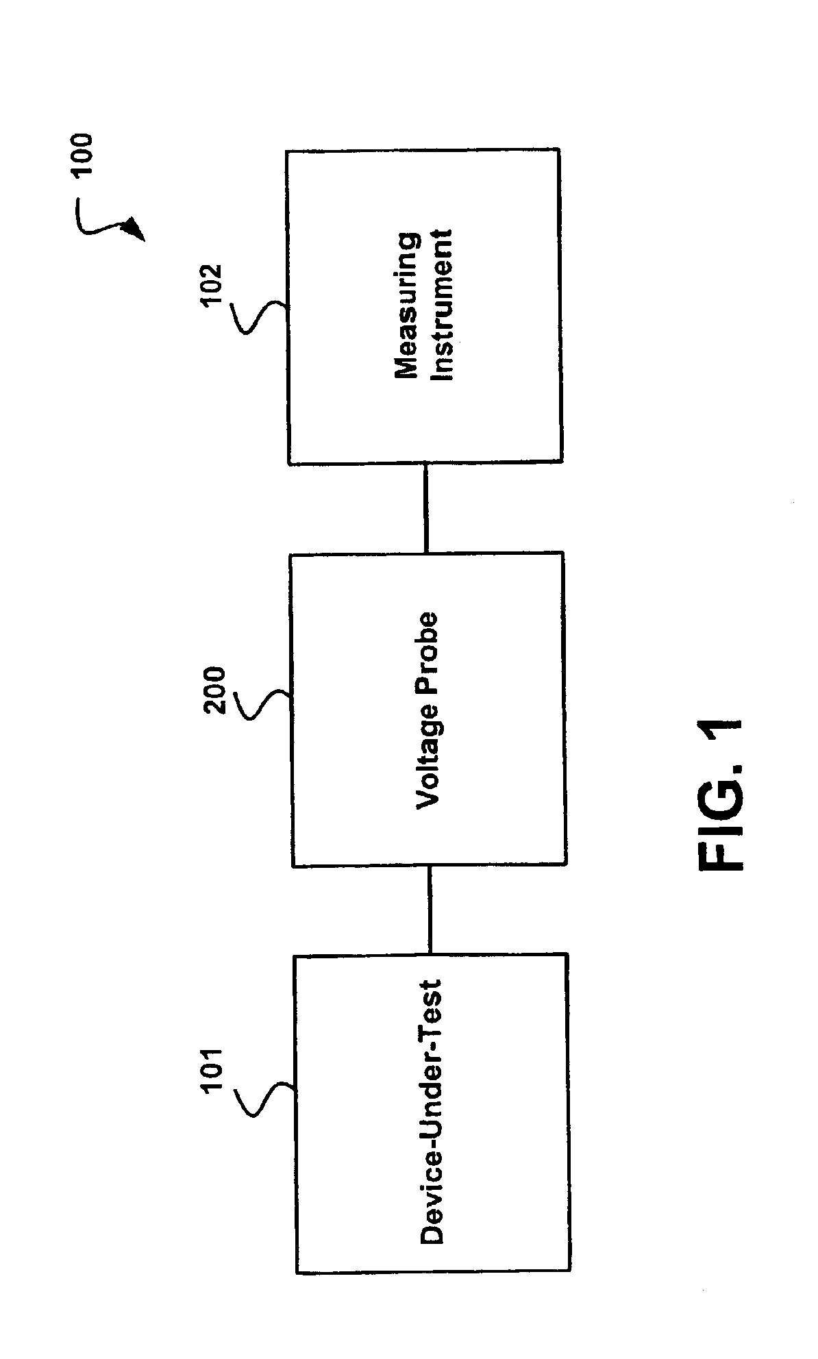
FIG. 1 is a block diagram depicting an embodiment of a measurement system 100 according to the present invention. The measurement system 100 includes a differential voltage probe 200 that is coupled to a measuring instrument 102 and to a device-under-test 101. The device-under-test 101 may be, for example, an electronic device or circuit that is to be tested. The probe 200 is configured to provide the measuring instrument 102 with probe signals that are responsive to input signals received by the probe 200 from the device-under-test 101. The measuring instrument 102 is configured to measure one or more characteristics of probe signals received from the probe 200. The measuring instrument 102 may be, for example, an oscilloscope, a spectrum analyzer, a logic analyzer, a vector analyzer, a network analyzer, or a time interval analyzer, among others.

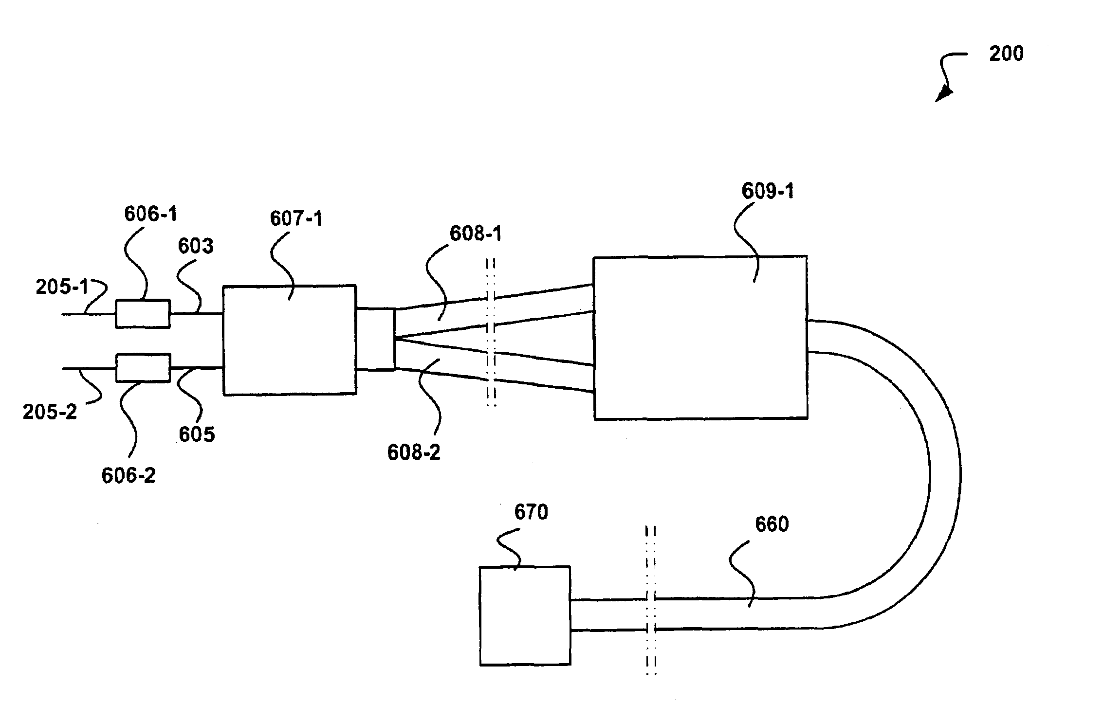
FIG. 2 is a block diagram depicting an embodiment of selected components of a voltage probe 200, according to the present invention. The v...


PUM


Abstract

A voltage probe includes a first signal lead configured to receive a first signal from a device under test, a first probe-tip network that is coupled to the first signal lead and that has a frequency response that includes a first transmission zero, a first compensation network that is coupled to the first probe-tip network and that has a frequency response that includes a first transmission pole, a second signal lead configured to receive a second signal from the device under test, a second probe-tip network that is coupled to the second signal lead and that has a frequency response that includes a second transmission zero, a second compensation network that is coupled to the second probe-tip network and that has a frequency response that includes a second transmission pole, and a differential amplifier circuit that is coupled to the first compensation network and to the second compensation network, and that is configured to provide a third signal that is responsive to the first signal and to the second signal. Methods and other systems for providing electrical connections to devices under test are disclosed.

Description

DESCRIPTION OF THE RELATED ARTThe frequency response of a measurement of a signal is dependent upon the capacitance of a probe in parallel with the source impedance of the point being probed. The capacitive reactance of the probe varies as a function of frequency, thereby causing the impedance of the probe to also vary with frequency. This variation limits the accuracy of a probe measurement because the impedance of the probe falls substantially at high frequencies. One approach for extending the effective bandwidth of a probe has been to compensate for the capacitance of a probe by using active electronics at the probe tip. However, this has typically caused a probe tip to be bulky and easily damaged.The usefulness of a voltage probe depends upon the range of frequencies for which the response is true to the detected signal, the accuracy of replication, and the extent to which the probe detects the signal without detrimentally affecting the operation of the system or circuit being ...

Claims


Application Information

Patent Timeline
Patent Type & Authority Patents(United States)
IPC IPC(8): G01R1/06G01R27/26G01R27/08G01R31/02G01R1/067
CPCG01R1/06766
Inventor MCTIGUE, MICHAEL T.RUSH, KENNETHKIMURA, BOBLUJAN, MICHAEL J.
Owner AGILENT TECH INC
Why Eureka
Try Eureka