Multi-layer microfluidic devices

a microfluidic device and multi-layer technology, applied in the direction of diaphragms, fluid speed measurement, valve details, etc., can solve the problem of limiting the size of the microfluidic device produced in this manner, and achieve the effect of further reducing the size of the microfluidic devi

Inactive Publication Date: 2005-02-22
CAPLIPER LIFE SCI INC
View PDF46 Cites 155 Cited by
  • Summary
  • Abstract
  • Description
  • Claims
  • Application Information

AI Technical Summary

Benefits of technology

In a more specific embodiment, the multi-layer devices of the invention are useful in methods of sequencing nucleic acids. In particular, the devices for this application typically include at least five substrate layers. The devices also include at least four separation channels, each of the separation channels disposed between two different substrate layers. A common sample reservoir is included, connected to each of the four separation channels via fo

Problems solved by technology

While these microfabrication techniques permit the incorporation of relatively complex channel networks in a relatively small area, the ability to furth

Method used


Image

  • Multi-layer microfluidic devices
  • Multi-layer microfluidic devices
  • Multi-layer microfluidic devices

Examples


Embodiment Construction

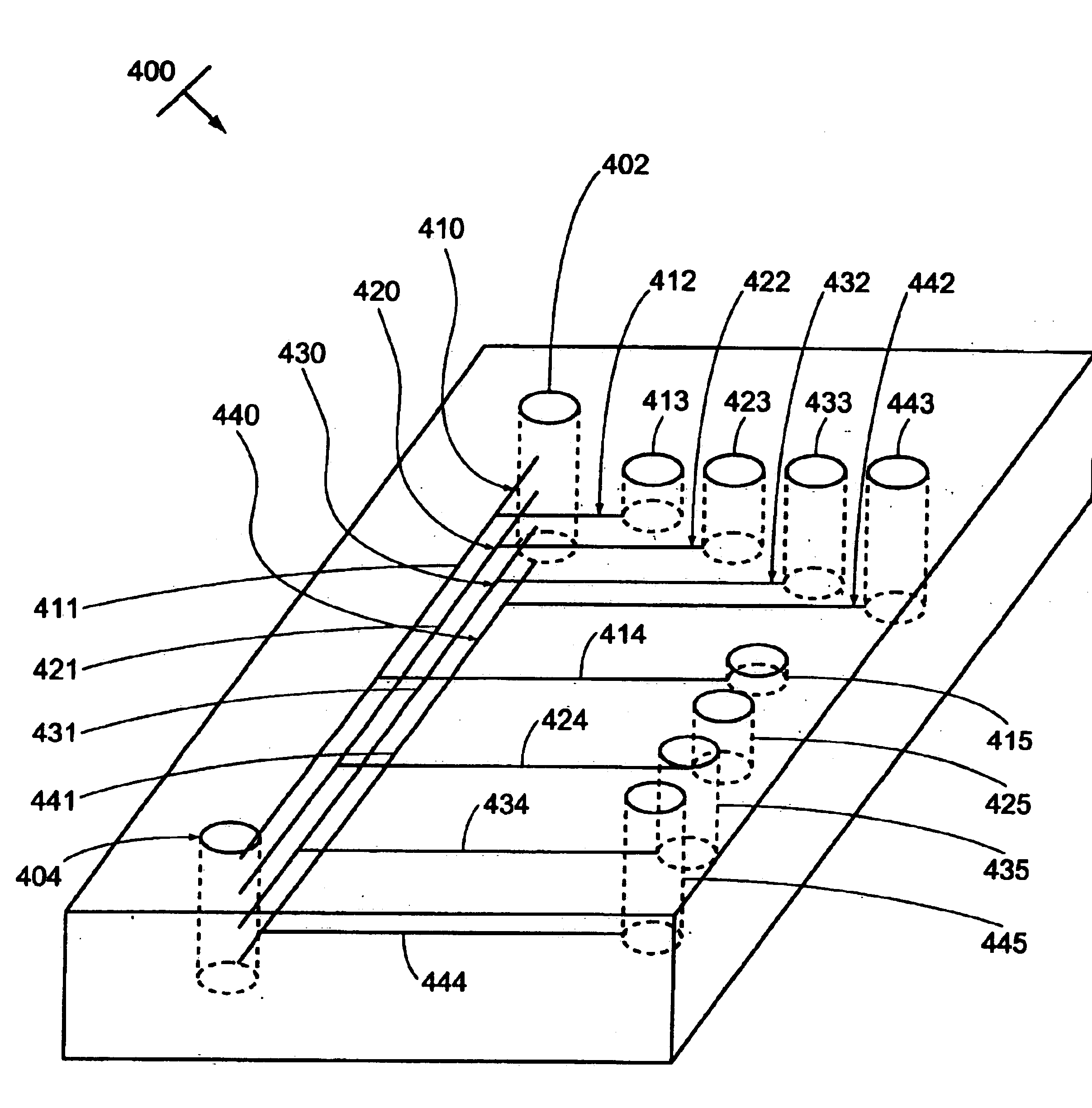
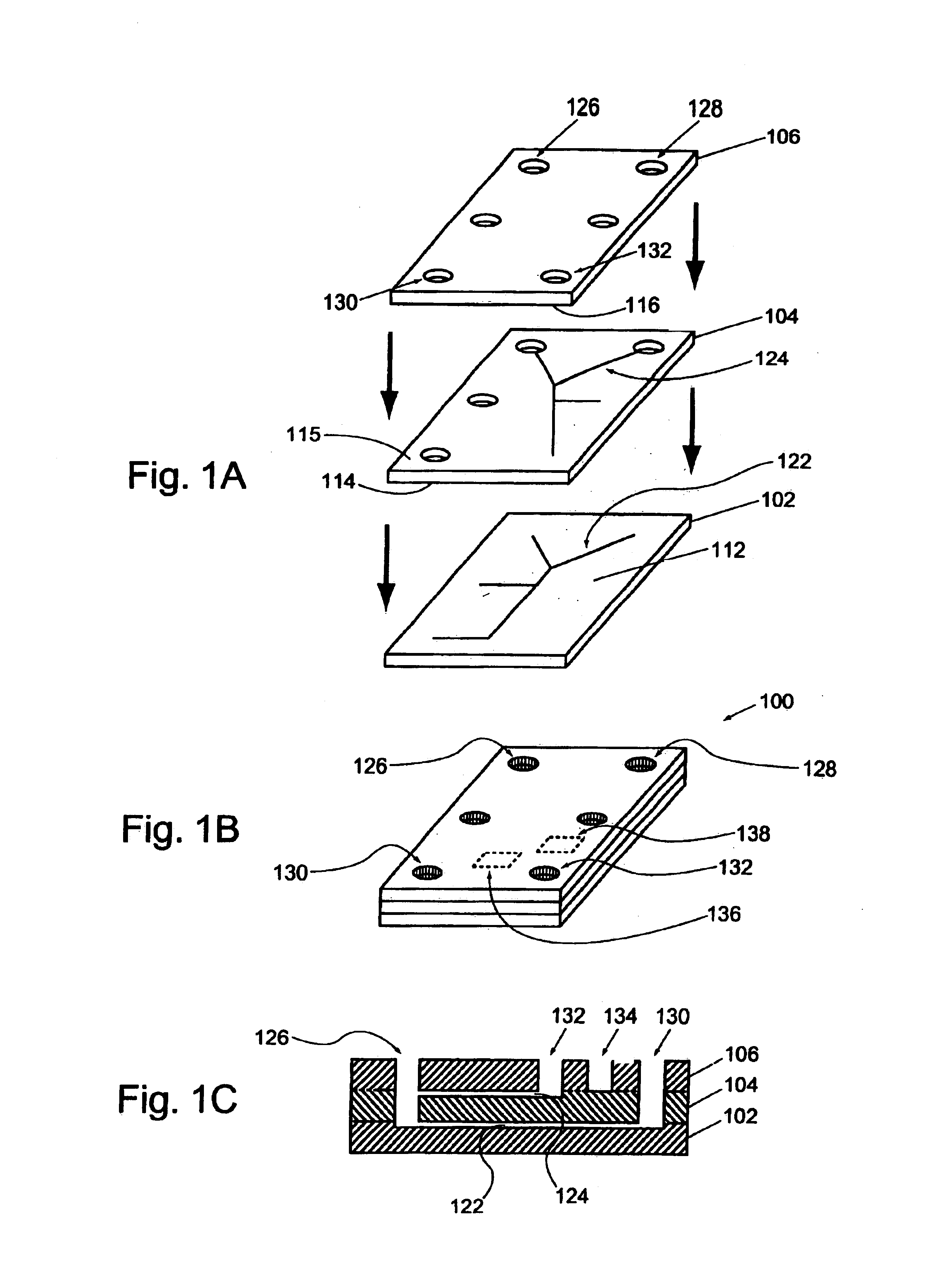
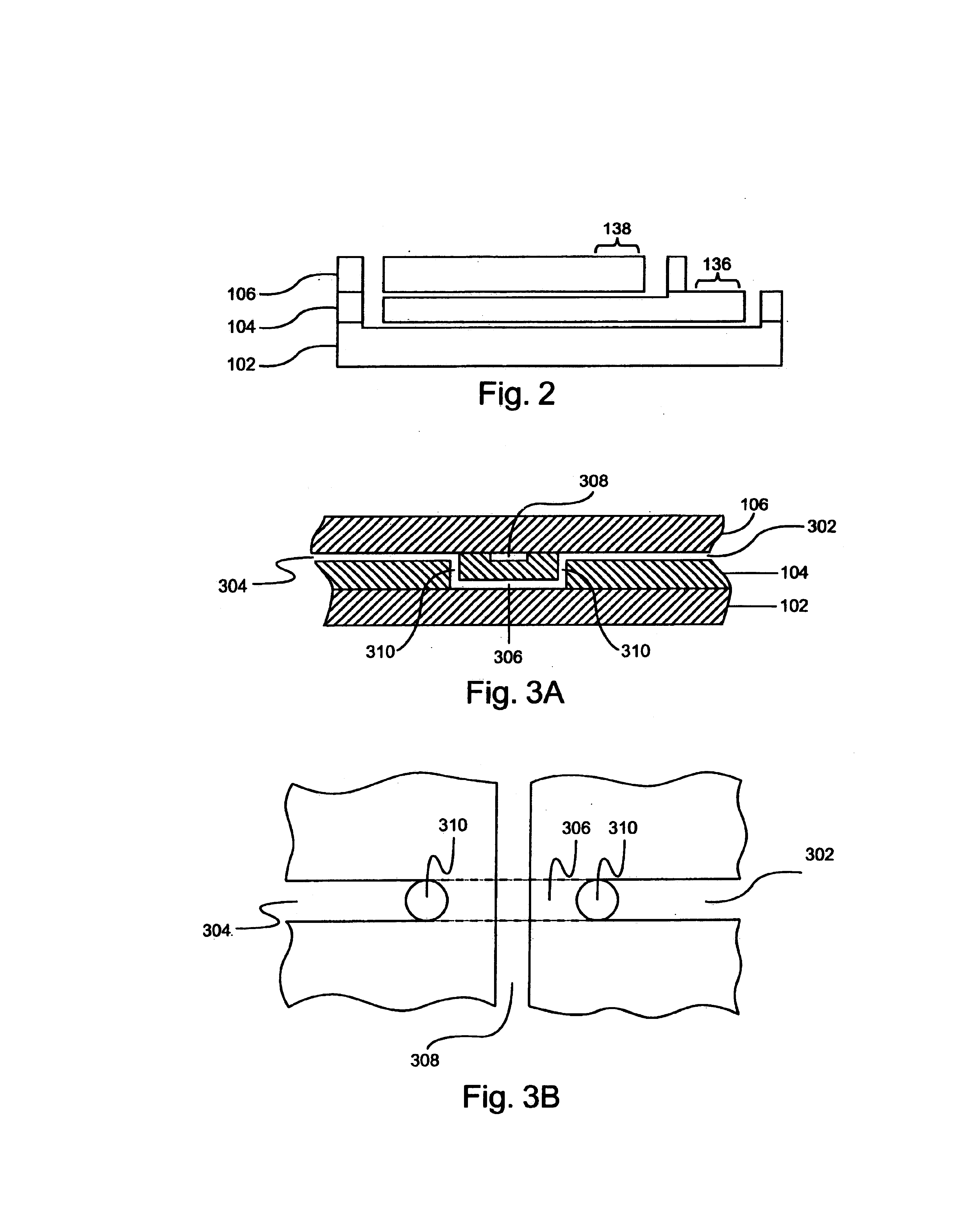
In most instances, microfluidic devices have been manufactured using microfabrication methods commonly employed in the electronics industry. Such methods generally involve the fabrication of microscale structures, e.g., grooves, wells, depressions and the like, on the upper planar surface of a first solid substrate material. A second substrate layer having a lower planar surface is then bonded over this surface, which covers and seals the grooves and wells to form the channels and chambers. As a result of these manufacturing techniques, microfluidic devices most often employ a planar structure where, aside from their intrinsic depth, the fluidic elements generally exist in two dimensions. The present invention, on the other hand, provides three dimensional microfluidic devices, e.g., employing multi-layered channel structures and networks. By providing multiple layers, the present invention provides a large number of advantages over previously described systems. For example, by prov...


PUM


Abstract

The present invention provides multi-layer microfluidic systems, by providing additional substrate layers, e.g., third, fourth, fifth and more substrate layers, mated with the typically described first and second layers. Microfabricated elements, e.g., grooves, wells and the like, are manufactured into the surfaces between the various substrate layers. These microfabricated elements define the various microfluidic aspects or structures of the overall device, e.g., channels, chambers and the like. In preferred aspects, a separate microscale channel network is provided between each of the substrate layers.

Description

BACKGROUND OF THE INVENTIONMicrofluidic devices and systems have been gaining increasing interest for their ability to provide improved methods of performing chemical, biochemical and biological analysis and synthesis. In particular, the small size and automatability of these microfluidic systems provides a variety of advantages in terms of low reagent requirements, low space requirements, shorter reaction times, and integratability. All of these advantages together, provide systems which can be extremely useful in performing large numbers of reactions in parallel, in order to provide enhanced analytical throughput.In general, the production of microfluidic devices has been enabled by advancements in microfabrication technology used in the electronics and semiconductor manufacturing industries. Specifically, technologies, such as photolithography, wet chemical etching, injection molding of plastics, and the like, have been used to fabricate microscale channels and wells in the surfa...

Claims


Application Information

Patent Timeline
IPC IPC(8): B01L3/00B01J19/00B81B1/00C40B60/14
CPCB01J19/0093B01L3/5027B81B1/004C40B60/14B01J2219/00351B01J2219/00587B01J2219/00702B01L2300/0816B01L2300/0864B01L2300/0874B01L2300/0887B01L2400/0415B01L2400/0487B81B2201/0214B81B2201/058B01J2219/00317Y10T137/2224Y10T137/8242Y10T137/8326
Inventor CHOW, CALVIN Y. H.
Owner CAPLIPER LIFE SCI INC
Why Eureka
Try Eureka