Bonding pad metal layer geometry design

a technology of metal layer geometry and bonding pad, which is applied in the direction of semiconductor devices, semiconductor/solid-state device details, electrical equipment, etc., can solve the problems of high stress concentration of bonding pad corners, unfavorable yield effect, and carpeting and imd cracking of bonding pads, etc., to achieve the effect of relieving stress

Inactive Publication Date: 2005-02-22
TAIWAN SEMICON MFG CO LTD
View PDF6 Cites 21 Cited by
  • Summary
  • Abstract
  • Description
  • Claims
  • Application Information

AI Technical Summary

Benefits of technology

A bonding pad suitable for use in wire bonding an integrated circuit includes an approximately rectangular metal pattern. The bonding pad has at least o...

Problems solved by technology

In this type of pad, the bonding pad corner has a high stress concentration and often peels or lifts up during wire bonding.
In addition...

Method used


Image

  • Bonding pad metal layer geometry design
  • Bonding pad metal layer geometry design
  • Bonding pad metal layer geometry design

Examples


Embodiment Construction

The present invention is embodied in a bonding pad, an integrated circuit package including the bonding pad, and a method for forming an integrated circuit package using the bonding pad. The exemplary bonding pads reduce corner stress and increase adhesion against pad peeling.

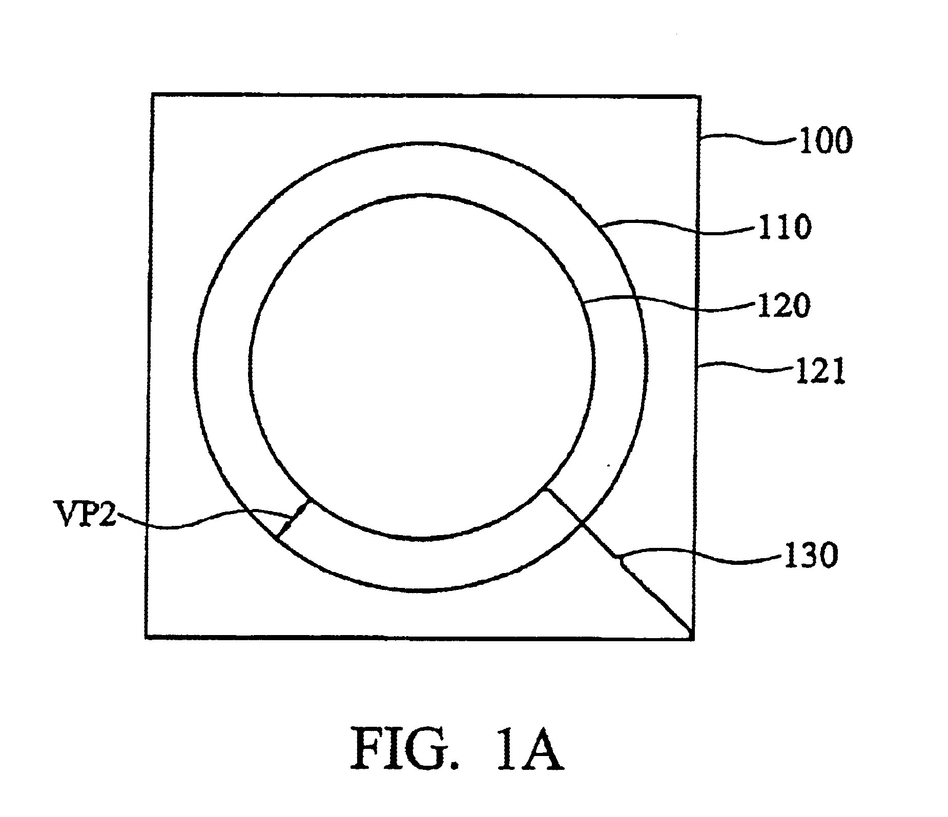
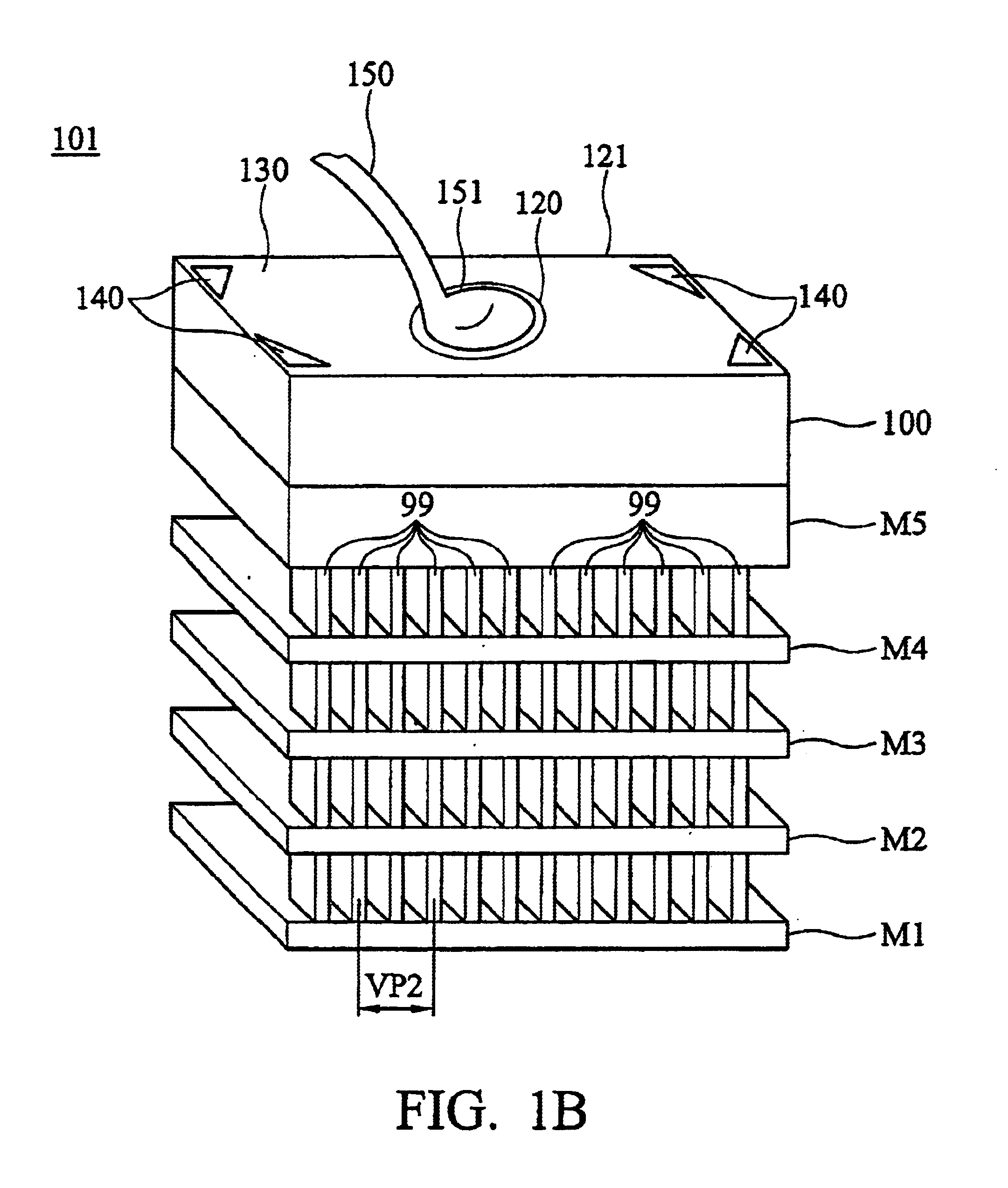
FIG. 1A shows an exemplary bonding pad 100. The bonding pad 100 has a wire bond ball area 110. An inner or central portion 120 of the bonding pad 100 is designated as a solid pattern area. A solid pattern of metal is deposited in region 120. The region 130 between the circumference of the solid pattern area 120 and the perimeter 121 of the bonding pad 100 is designated as a slot / hole area, in which a plurality of slots or holes are formed in the bonding pad metal. The slot / hole area 130 has a minimum dimension of at least VP2, where VP2 is twice the minimum pitch between vias (best seen in FIG. 1B).

FIG. 1B shows a representative set of layers in a semiconductor integrated circuit device 101. A plurality of meta...


PUM


Abstract

A bonding pad suitable for use in wire bonding an integrated circuit includes an approximately rectangular metal pattern. The bonding pad has at least one slot or hole in it, located at or adjacent to at least one corner of the approximately rectangular metal pattern. The slot or hole provides peeling stress relief.

Description

FIELD OF THE INVENTIONThe present invention relates to semiconductor packages generally, and more specifically to bonding pads for wire bonding.BACKGROUND OF THE INVENTIONDuring the fabrication of an integrated circuit package, a die containing a plurality of circuit patterns is connected to an integrated circuit package substrate. The package substrate has a plurality of pins for connecting the circuitry to an external printed wiring board.The most common method for forming electrical connections between the die and the package substrate is wire bonding. A plurality of bonding pads is located around the perimeter on a top surface of the die. A corresponding set of contacts is located on the package substrate. A plurality of connecting wires are bonded to connect each bonding pad to a respective contact on the package substrate, using a method such as ultrasonic bonding. Following wire bonding, the package is encapsulated and sealed.Traditional bonding pads have the same shape as th...

Claims


Application Information

Patent Timeline
IPC IPC(8): H01L23/485H01L23/48
CPCH01L24/05H01L24/48H01L24/45H01L2924/00014H01L2924/01033H01L2924/01023H01L2924/14H01L2924/01079H01L2224/85399H01L2224/48599H01L2224/48463H01L2224/45144H01L2224/04042H01L2224/05093H01L2224/05096H01L2224/05556H01L2224/05599
Inventor HUANG, TAI-CHUNLEE, TZE-LIANG
Owner TAIWAN SEMICON MFG CO LTD
Why Eureka
Try Eureka