
Organic electroluminescence display device having sealing structure and method of fabricating the same

a technology sealing structure, which is applied in the direction of discharge tube luminescnet screen, discharge tube/lamp details, electric discharge lamps, etc., can solve the problems of large cathode ray tube size, high driving voltage, and malfunction of organic electroluminescence display device, and achieve the effect of long lifetim

Inactive Publication Date: 2005-03-01
LG DISPLAY CO LTD
View PDF3 Cites 36 Cited by
  • Summary
  • Abstract
  • Description
  • Claims
  • Application Information

AI Technical Summary

Benefits of technology

Another object of the present invention is to provide an organic electroluminescence display device and a method of fabricating the same that provides long lifetime.
Another object of the present invention is to provide an organic electroluminescence display device and a method of fabricating the same that is reliable.

Problems solved by technology

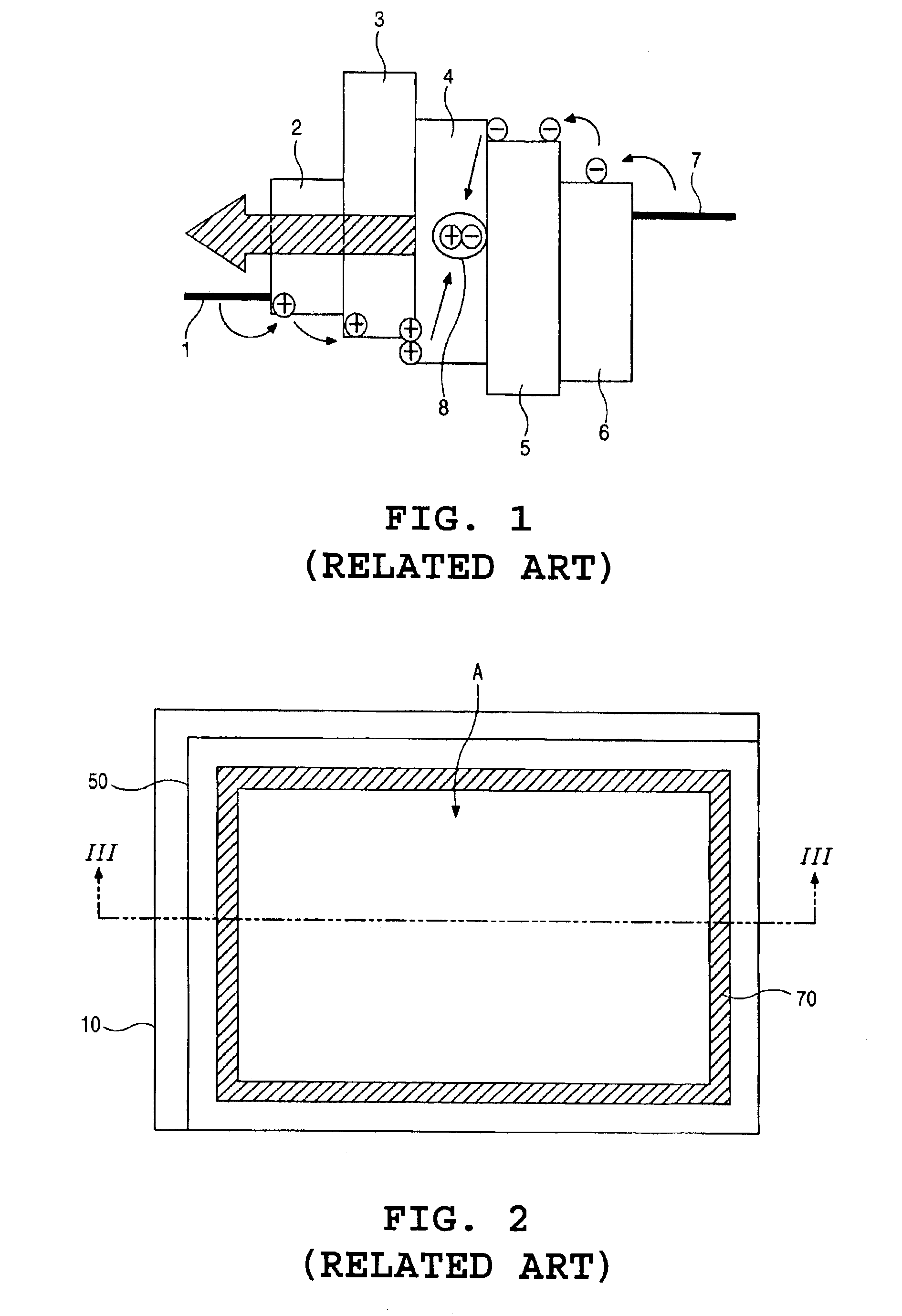
However, the cathode ray tube has large size, heavy weight, and high driving voltage.
Therefore, it causes malfunction of the organic electroluminescence display device, and a lifetime of the organic electroluminescence display device is reduced significantly.

Method used


Image

  • Organic electroluminescence display device having sealing structure and method of fabricating the same
  • Organic electroluminescence display device having sealing structure and method of fabricating the same
  • Organic electroluminescence display device having sealing structure and method of fabricating the same

Examples


Embodiment Construction

Reference will now be made in detail to the illustrated embodiments of the present invention, examples of which are illustrated in the accompanying drawings. Wherever possible, the same reference numbers will be used throughout the drawings to refer to the same or like parts.

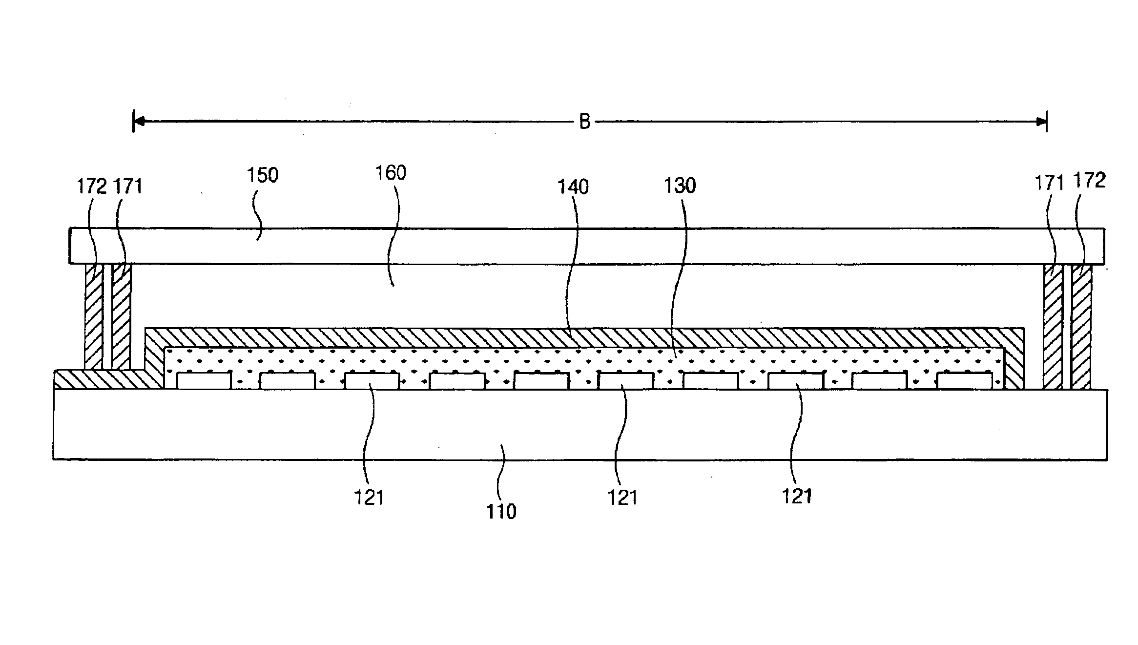
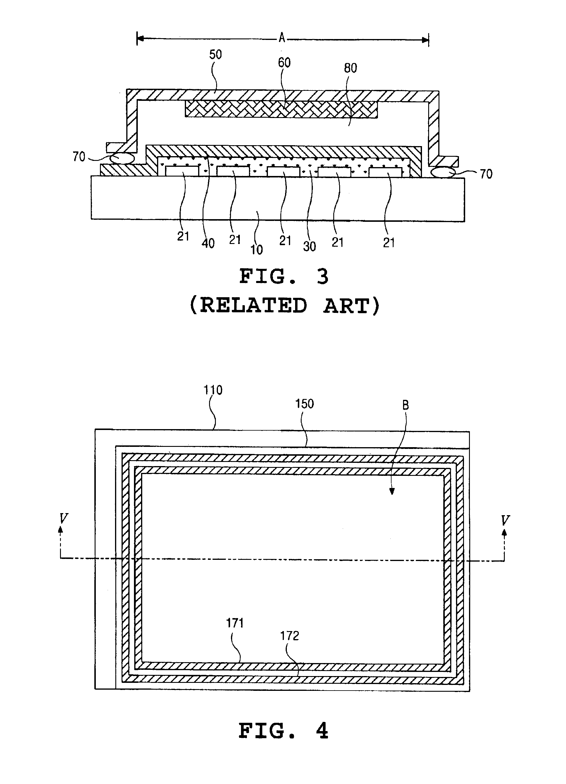
FIG. 4 is a schematic plane view of an organic electroluminescence display device according to the present invention. As shown in FIG. 4, the organic electroluminescence display device includes a first substrate 110 and a second substrate 150. The second substrate 150 has a smaller area than the first substrate 110 and exposes a part of the first substrate 110. First and second sealants 171 and 172 are formed between the first and second substrates 110 and 150, and define an array region “B”. The second sealant 172 surrounds the first sealant 171.

FIG. 5 is a cross-sectional view of the organic electroluminescence display taken along the line V—V of FIG. 4.

In FIG. 5, a plurality of anode electrodes 121 are formed...


PUM


Abstract

An organic electroluminescence display device and a method of fabricating the same are disclosed in the present invention. The organic electroluminescence display device includes a substrate, a sealing element spaced apart from the substrate, a first sealant disposed between the substrate and the sealing element, the first sealant defining an array region and an airtight space between the substrate and the sealing element, a second sealant disposed between the substrate and the sealing element, the second sealant surrounding the first sealant, a first electrode in the array region on an inner surface of the substrate, an emissive layer on the first electrode, and a second electrode on the emissive layer.

Description

This application claims the benefit of the Korean Patent Application No. P2001-087425 filed on Dec. 28, 2001, which is hereby incorporated by reference.BACKGROUND OF THE INVENTION1. Field of the InventionThe present invention relates to an electroluminescence display device, and more particularly, to an organic electroluminescence display device and a method of fabricating the same. Although the present invention is suitable for a wide scope of applications, it is particularly suitable for fabricating a reliable electroluminescence display device.2. Discussion of the Related ArtA cathode ray tube has been widely used as a display device such as a television and a computer monitor. However, the cathode ray tube has large size, heavy weight, and high driving voltage. Therefore, flat panel displays having characteristics of being thin, light weight, and low in power consumption have been in demand. The flat panel displays include a liquid crystal display device, a plasma display panel ...

Claims


Application Information

Patent Timeline
IPC IPC(8): H01L51/52H01L51/50H05B33/04
CPCH01L51/5237H10K50/8426H10K59/8722H05B33/04
Inventor KIM, KWAN-SOOPARK, JAE-YONG
Owner LG DISPLAY CO LTD
Learn More