Device for compensating for a test temperature deviation in a semiconductor device handler

Inactive Publication Date: 2005-03-01
MIRAE CORPORATION
View PDF6 Cites 94 Cited by
  • Summary
  • Abstract
  • Description
  • Claims
  • Application Information

AI Technical Summary

Benefits of technology

Accordingly, the invention is directed to a device for compensating for a test temperature deviation in a handler that substantially obviates one or more of the problems due to limitations and disadvantages of the related art.
To achieve these and other advantages and in accordance with the purpose of the present invention, as embodied and broadly described, a semiconductor device handler is provided which includes at least one enclosed chamber, a heating/cooling apparatus configured to bring an inside of the at least one chamber to a low or high temperature state, a pushing unit provided within the at least on

Problems solved by technology

This added heat impedes conducting a test at an exact preset temperature.
This is a problem that must be solved for both test and actual application environments as the semiconductor devices become smaller and packing density increases.
For example, in a high temperature test, if a user sets a temperature of an inside of the chamber to 80° C. for the test, if there is no h

Method used


Image

  • Device for compensating for a test temperature deviation in a semiconductor device handler
  • Device for compensating for a test temperature deviation in a semiconductor device handler
  • Device for compensating for a test temperature deviation in a semiconductor device handler

Examples


Example

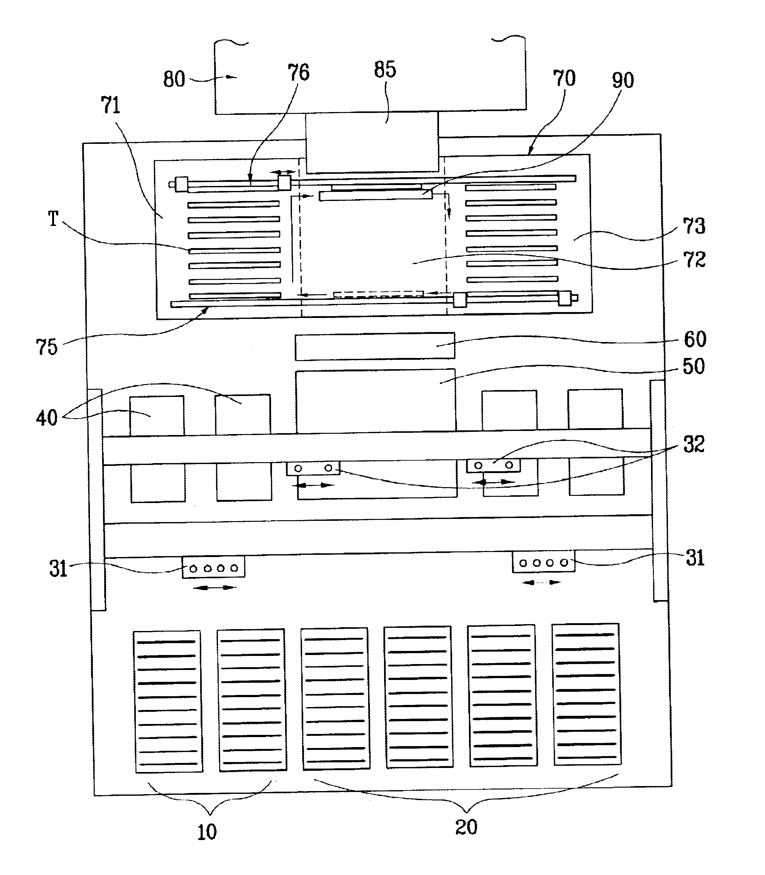
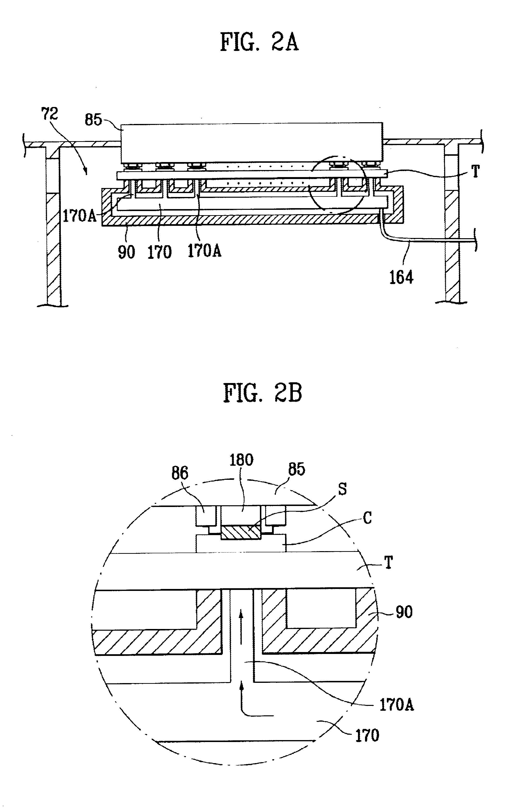
Reference will now be made in detail to the embodiments of the present invention, examples of which are illustrated in the accompanying drawings. FIG. 1 is a schematic plan view of a handler having a device for compensating a test temperature deviation in accordance with the invention. FIGS. 2A and 2B are schematic side sectional views of a test site of the handler of FIG. 1.

The handler and its operation will be explained as follows.

The handler shown in FIG. 1 includes a loading unit 10 in a front portion of the handler 1, in which user trays may be loaded, and an unloading unit 20 to one side of the loading unit 10, in which tested semiconductor devices may be loaded on the user trays, with the tested semiconductor devices classified according to a result of the test(s).

Buffer units 40 are provided on both sides of a middle position of the handler 1. The buffer units 40 temporarily retain the semiconductor devices transported from the loading unit 10. An exchange unit 50 is provide...


PUM


Abstract

A semiconductor device handler is provided, in which a test temperature deviation of a semiconductor device caused by heat produced by the semiconductor device itself during testing is compensated for, allowing a test of the semiconductor device to be carried out at an exact temperature, or within an exact temperature range. The semiconductor device handler includes at least one enclosed chamber, a heating/cooling apparatus configured to bring an inside of the at least one chamber to a low or high temperature state, a pushing unit provided within the at least one chamber and configured to push a plurality of semiconductor devices mounted on a test tray into test sockets of a test board located within the at least one chamber for testing, a cooling fluid supplying apparatus configured to supply cooling fluid, a nozzle assembly configured to spray cooling fluid received from the cooling fluid supplying apparatus onto the semiconductor devices fitted to the test sockets, and a control unit configured to control spraying of cooling fluid onto the semiconductor devices during testing to compensate for temperature changes of the semiconductor devices that occur during testing.

Description

BACKGROUND OF THE INVENTION1. Field of the InventionThe invention relates to a handler for use in testing semiconductor devices, and more particularly, to a device for compensating for a test temperature deviation in a semiconductor device handler.2. Background of the Related ArtIn general, memory, or non-memory semiconductor devices, or modules each having memory, and / or non-memory semiconductor devices arranged on a substrate to form a circuit, are subjected to various tests after fabrication before shipment. The semiconductor device handler (hereafter referred to as “handler”) is an apparatus for automatic transportation of the semiconductor devices or the modules during testing. The handler carries out a process in which, when a loading stacker receives trays having the semiconductor devices or modules held therein, a picker robot transports the semiconductor devices or modules to be tested to a test site, fits them into test sockets, carries out required tests, transports the t...

Claims


Application Information

Patent Timeline
IPC IPC(8): G01R1/00G01R1/44G01R31/28G01R31/26
CPCG01R31/2877G01R31/2862G01R31/2867
Inventor SONG, JAE MYEONGHAM, CHUL HOPARK, CHAN HOHWANG, EUI SUNGLIM, WOO YOUNGSEO, JAE BONGLEE, EUNG YONGLEE, BYENG GI
Owner MIRAE CORPORATION
Why Eureka
Try Eureka