

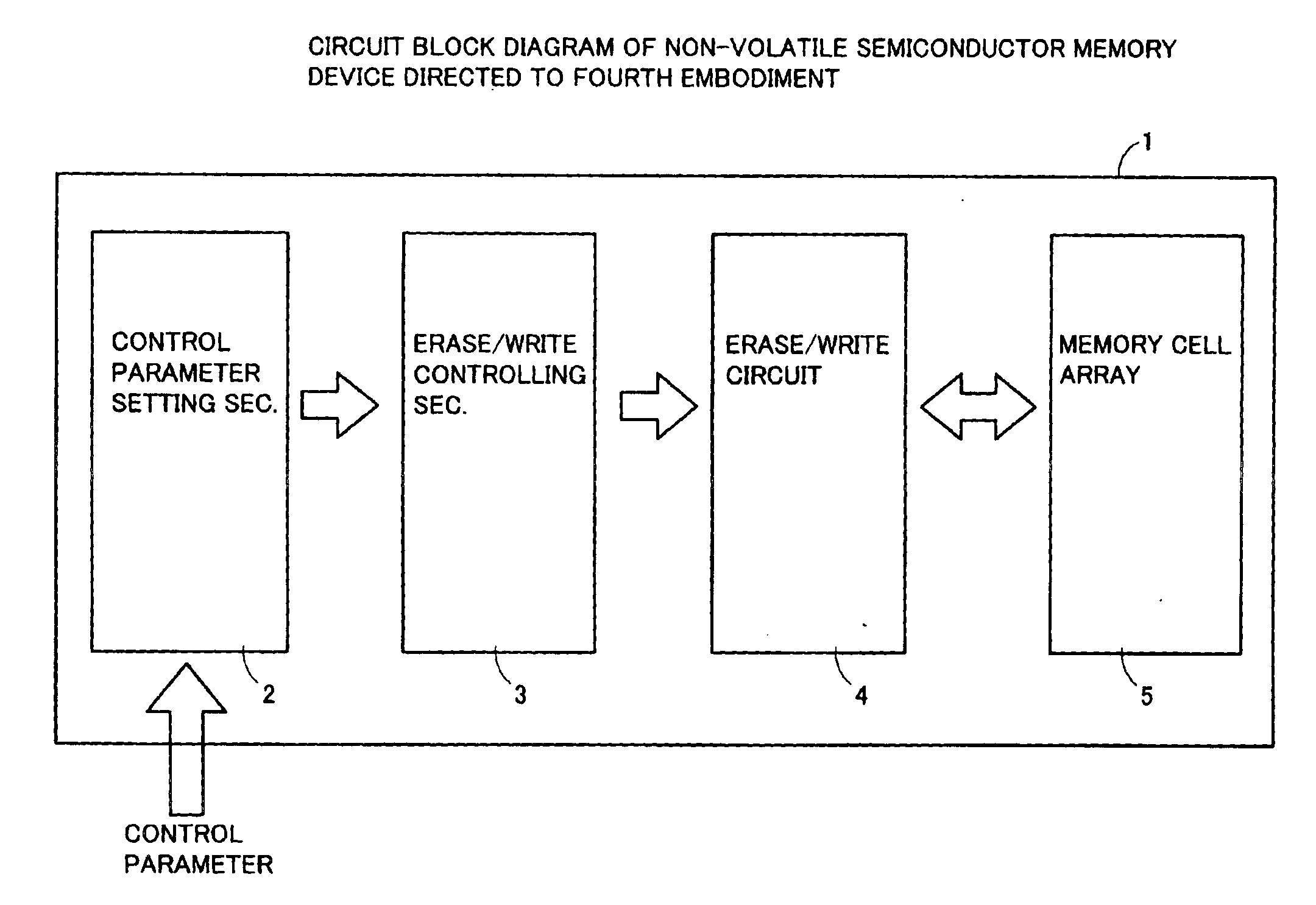
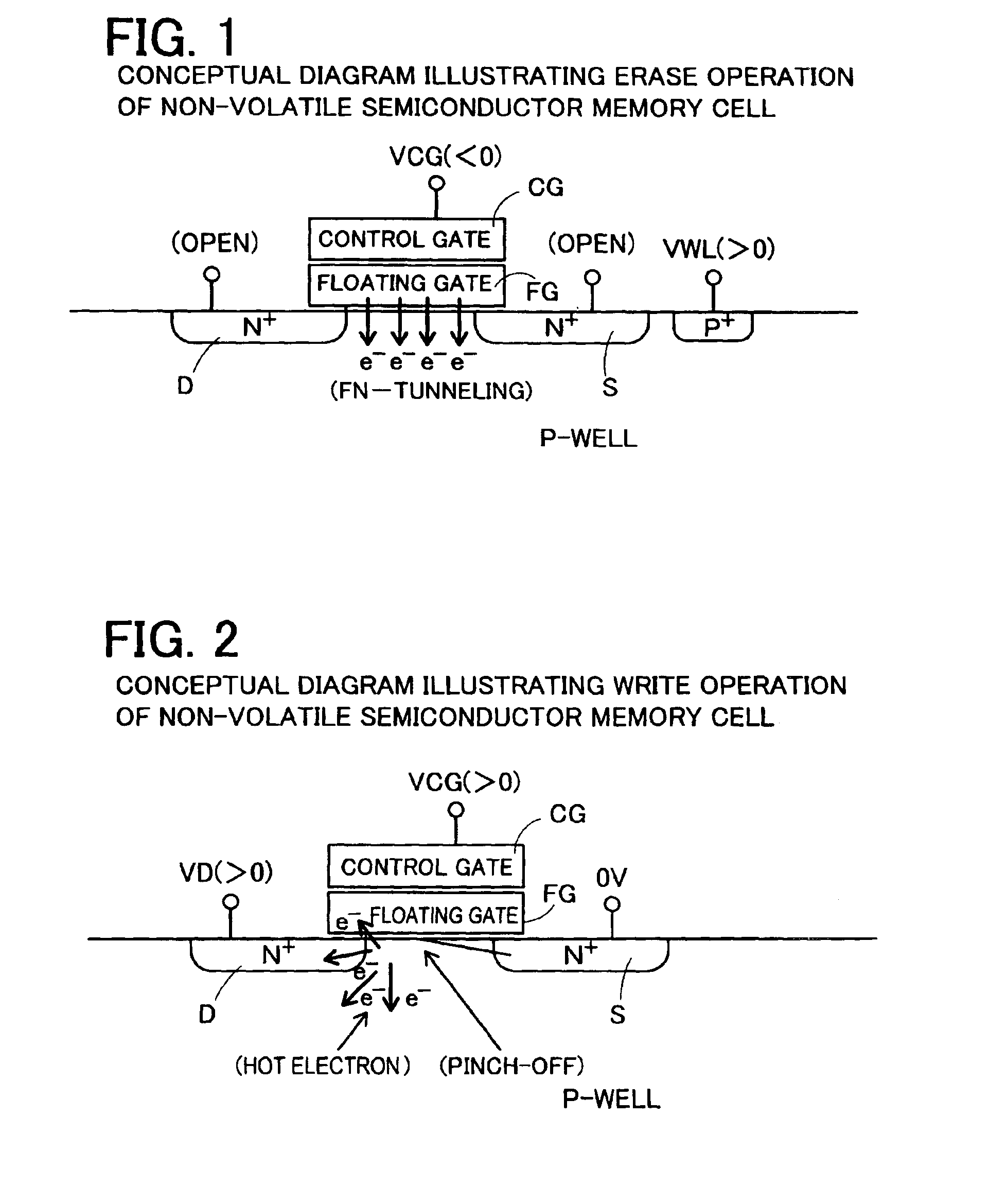
Control method of non-volatile semiconductor memory cell and non-volatile semiconductor memory device
a non-volatile semiconductor and memory cell technology, applied in the direction of digital storage, instruments, transistors, etc., can solve the problems of device reliability, erase operation cannot be efficiently conducted, and device reliability is problematic, and achieve the effect of high speed
Active Publication Date: 2005-03-01
MONTEREY RES LLC
View PDF8 Cites 29 Cited by
- Summary
- Abstract
- Description
- Claims
- Application Information
AI Technical Summary
Benefits of technology
[0016]The present invention has been made to solve at least one of the above described problems. Accordingly, it is an object of the present invention to provide control method and a non-volatile semiconductor memory device capable of erase operation or write operation in high speed securing reliability without applying excessive electric field.
Problems solved by technology
That is, this is to apply excessive electric field to a non-volatile semiconductor memory cell, which is problematic in terms of device reliability.
As a result, an erase operation cannot be conducted efficiently.
This is problematic in terms of device reliability.
Method used
View moreImage
Smart ImageViewing Examples

Examples
first embodiment
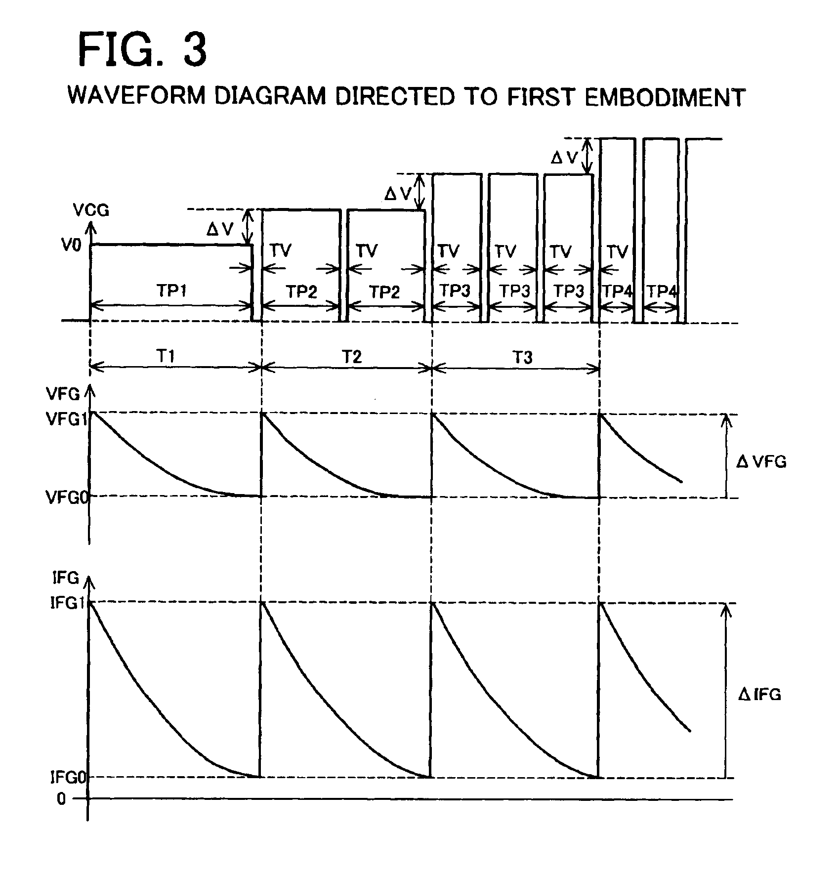
[0035]FIG. 3 is a waveform diagram directed to first embodiment;
[0036]FIG. 4 is a waveform diagram directed to variant of first embodiment;
second embodiment
[0037]FIG. 5 is a waveform diagram directed to second embodiment;
third embodiment
[0038]FIG. 6 is a waveform diagram directed to third embodiment;
Login to View More PUM
 Abstract
It is intended to provide control method and a nonvolatile semiconductor memory device capable of erase operation or write operation in high speed securing reliability without applying excessive electric field. An operation unit consists of a plurality of operation cycles each of which has a bias-application period and a verification period. Addition voltage ΔV is added to each operation unit as bias voltage, whereby a write operation can be carried out with characteristic of injected current IFG that is uniform among respective operation units duration of which are generally same. In this case, duration of operation cycles are shortened by each operation unit and duration of verification periods are shortened so as to avoid a situation such that a write operation completes in the middle of a bias-application period and after that, another write operation continues to cause excessive voltage stress on non-volatile semiconductor memory cells.
Description
CROSS-REFERENCE TO RELATED APPLICATIONS[0002]This application is based upon and claims the benefit of priority from each of the prior Japanese Patent Application No. 2002-274753 filed on Sep. 20, 2002, the entire contents of which are incorporated herein by reference.BACKGROUND OF THE INVENTION[0003]1. Field of the Invention[0004]The present invention relates to erase operation or write operation to a non-volatile semiconductor memory cell, more particularly, it relates to control method and a non-volatile semiconductor memory device capable of erase operation or write operation in high speed securing reliability.[0005]2. Description of Related Art[0006]Japanese Laid-open Patent Publication No. 11-39887 discloses a non-volatile semiconductor memory device that intends to shorten write operation time or the like. More particularly, the non-volatile semiconductor memory device improves ISPP method that raises pulse voltage by each applied cycle with respect to write pulse waveform so ...
Claims
Login to View More Application Information
Patent Timeline
 IPC IPC(8): G11C16/10G11C16/06G11C16/02H01L21/8247H01L27/10H01L27/115H01L29/788H01L29/792
CPCG11C16/10G11C16/3459G11C16/3445
InventorKAWABATA, SHOZO
OwnerMONTEREY RES LLC