Fabrication of trenches with multiple depths on the same substrate

a technology of trenches and substrates, applied in the direction of basic electric elements, semiconductor/solid-state device manufacturing, electric apparatus, etc., can solve the problems of reducing the processing efficiency affecting the patterning accuracy of the second trench, and affecting the quality of the second trench

Inactive Publication Date: 2005-03-08
BELL SEMICON LLC
View PDF3 Cites 90 Cited by
  • Summary
  • Abstract
  • Description
  • Claims
  • Application Information

AI Technical Summary

Benefits of technology

To achieve the foregoing, the present invention provides methods for fabrication of trenches with two or more depths on the same substrate. A stack having a pad oxide layer and a nitride (silicon nitride—Si3N4) layer is formed on the substrate. The wafer stack is covered with a resist layer and exposed with a first mask to form a preliminary trench. Using the mask, the preliminary trench is etched in the nitride film to a first depth corresponding to the

Problems solved by technology

One problem with forming field effect transistors on an SOI wafer is the floating body effect.
However, in SOI-CMOS technology the trench isolation completely separates devices from each other and does not permit a body contact.
Unfortunately, creation of two different trench depths on the same substrate is problematic.
However, patterning the second trench after defining the first trench is difficult, especially if the two trenches are contiguous or overlap.
Significant topography variation between the depth of the first trench and the surface of the substrate makes resist coverage difficult.
The

Method used


Image

  • Fabrication of trenches with multiple depths on the same substrate
  • Fabrication of trenches with multiple depths on the same substrate
  • Fabrication of trenches with multiple depths on the same substrate

Examples


Embodiment Construction

Reference will now be made in detail to preferred embodiments of the invention. Examples of the preferred embodiments are illustrated in the accompanying drawings. While the invention will be described in conjunction with these preferred embodiments, it will be understood that it is not intended to limit the invention to such preferred embodiments. On the contrary, it is intended to cover alternatives, modifications, and equivalents as may be included within the spirit and scope of the invention as defined by the appended claims. In the following description, numerous specific details are set forth in order to provide a thorough understanding of the present invention. The present invention may be practiced without some or all of these specific details. In other instances, well known process operations have not been described in detail in order not to unnecessarily obscure the present invention.

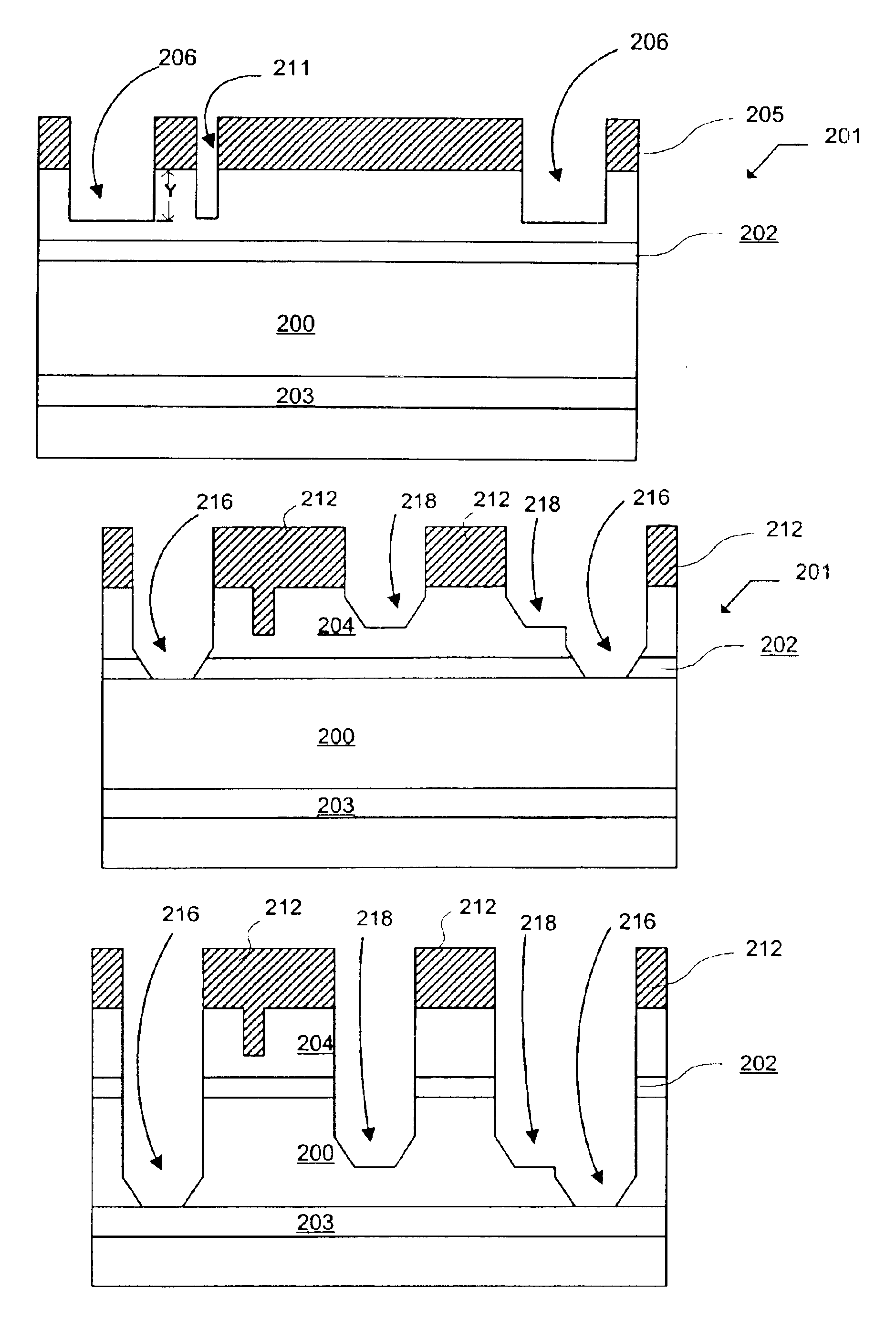
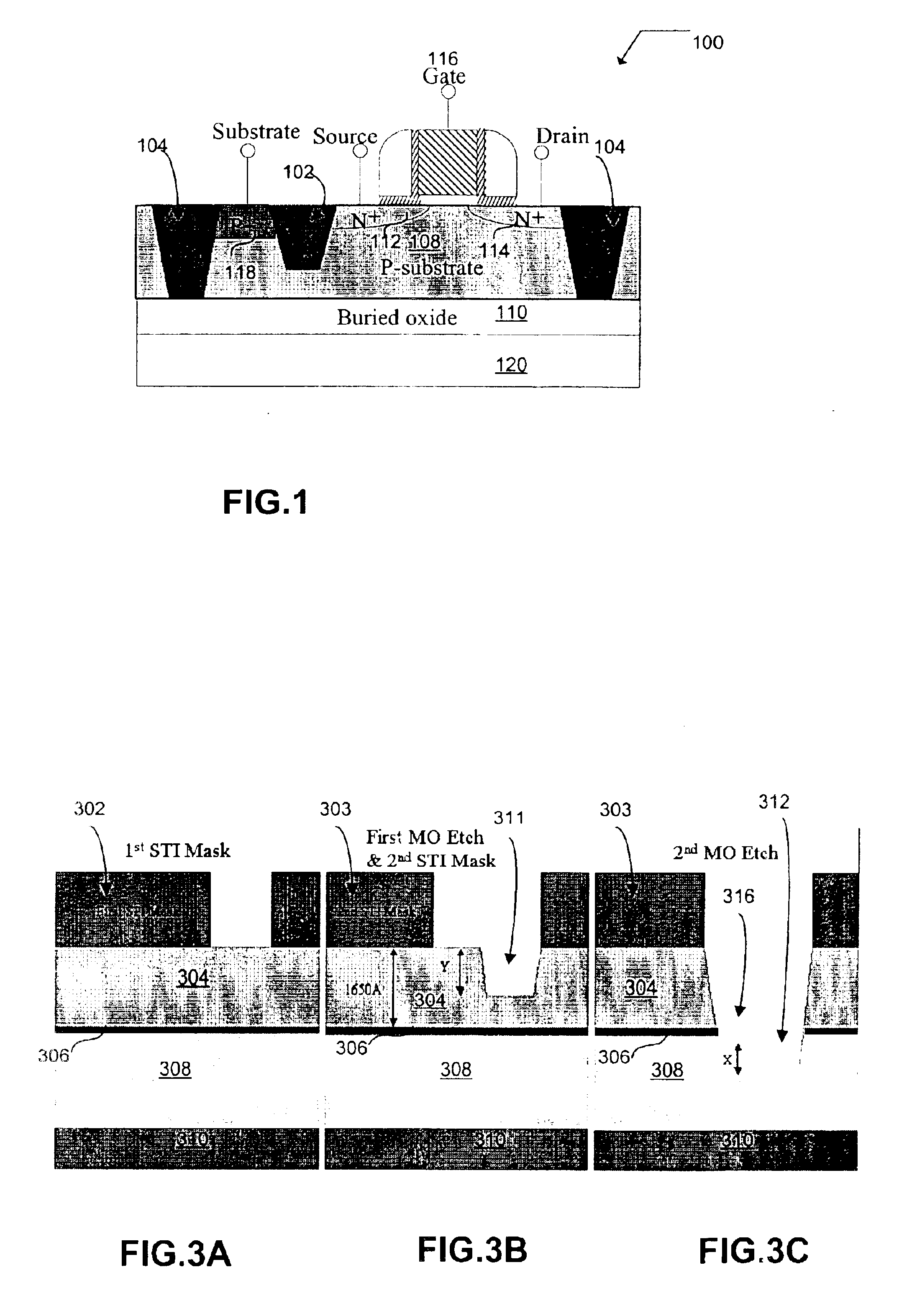
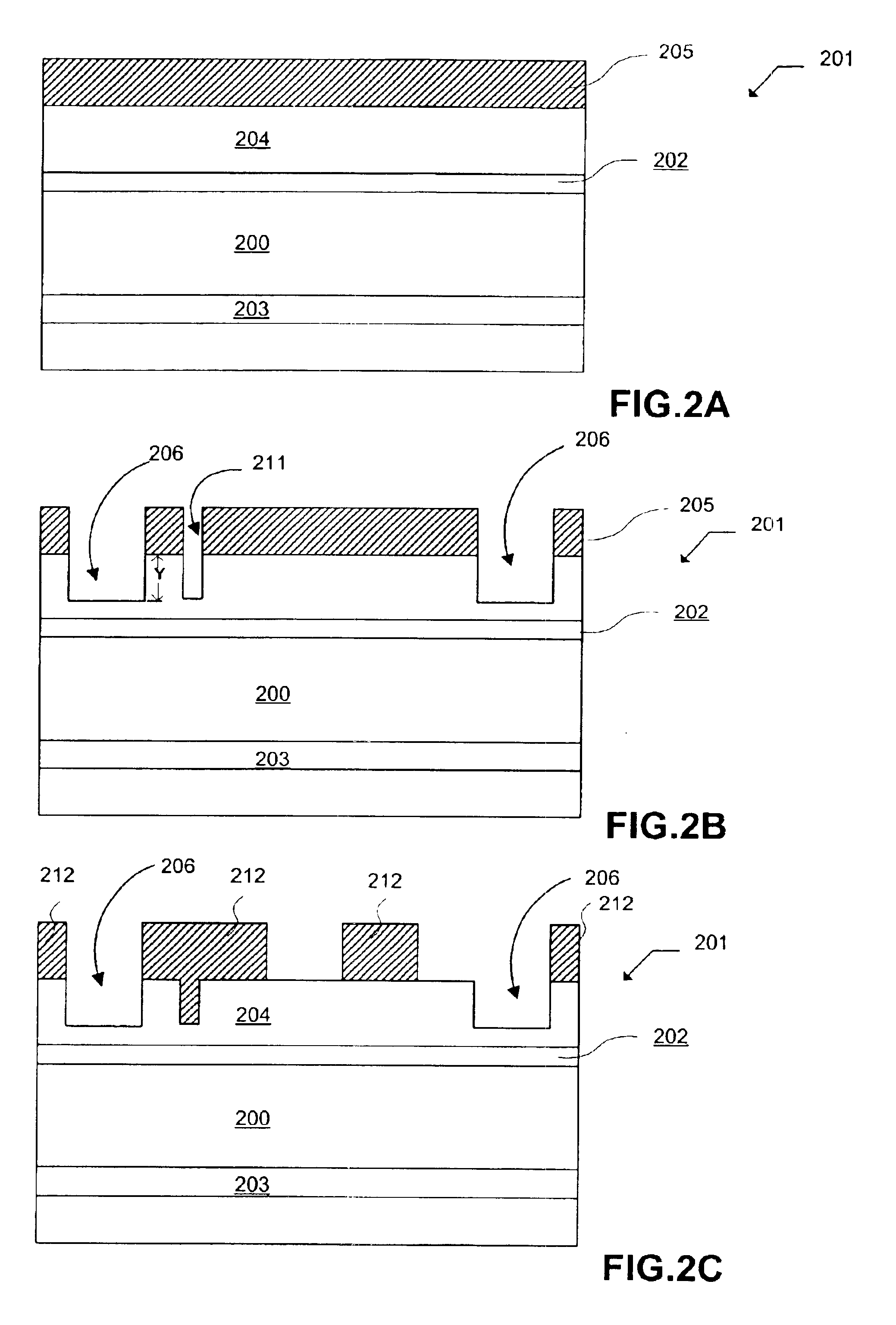
This invention offers an approach to achieve multiple trench depths on the same wafer by r...


PUM


Abstract

Dual trench depths are achieved on the same wafer by forming an initial trench having a depth corresponding to the difference in final depths of the shallow and deep trenches. A second mask is used to open areas for the deep trenches over the preliminary trenches and for the shallow trenches at additional locations. Etching of the shallow and deep trenches then proceeds simultaneously.

Description

BACKGROUND OF THE INVENTION1. Field of the InventionThe present invention relates to methods for fabricating integrated circuits with trenches. More particularly, the present invention relates to methods for forming trenches with multiple depths to isolate active device areas on SOI fabricated semiconductor wafers.2. Description of the Related ArtSemiconductor wafer fabrication involves a series of processes used to create semiconductor devices and integrated circuits (ICs) in and on a semiconductor wafer surface. Fabrication typically involves the basic operations of layering and patterning, together with others such as doping, and heat treatments. Layering is an operation used to add thin layers of material (typically insulator, semi-conductor or conductor) to the surface of the semiconductor wafer. Patterning is an operation that is used to remove specific portions of the top layer or layers on the wafer surface.Conventional or bulk semiconductor devices are formed in semiconduct...

Claims


Application Information

Patent Timeline
IPC IPC(8): H01L21/762H01L21/70
CPCH01L21/76229H01L21/76283H01L21/76232
Inventor MIRBEDINI, MOHAMMAD R.GOPINATH, VENKATESH P.LIN, HONGHORNBACK, VERNEDEFIBAUGH, DODDLE, YNHI
Owner BELL SEMICON LLC
Why Eureka
Try Eureka