

Method for manufacturing a semiconductor device
a manufacturing method and semiconductor technology, applied in semiconductor devices, semiconductor/solid-state device details, electrical devices, etc., can solve problems such as electric short-circuiting, signal transmission delay, and impediment to high-speed operations, and achieve excellent electric characteristics
- Summary
- Abstract
- Description
- Claims
- Application Information
AI Technical Summary
Benefits of technology
Problems solved by technology
Method used
Image

Examples
first embodiment
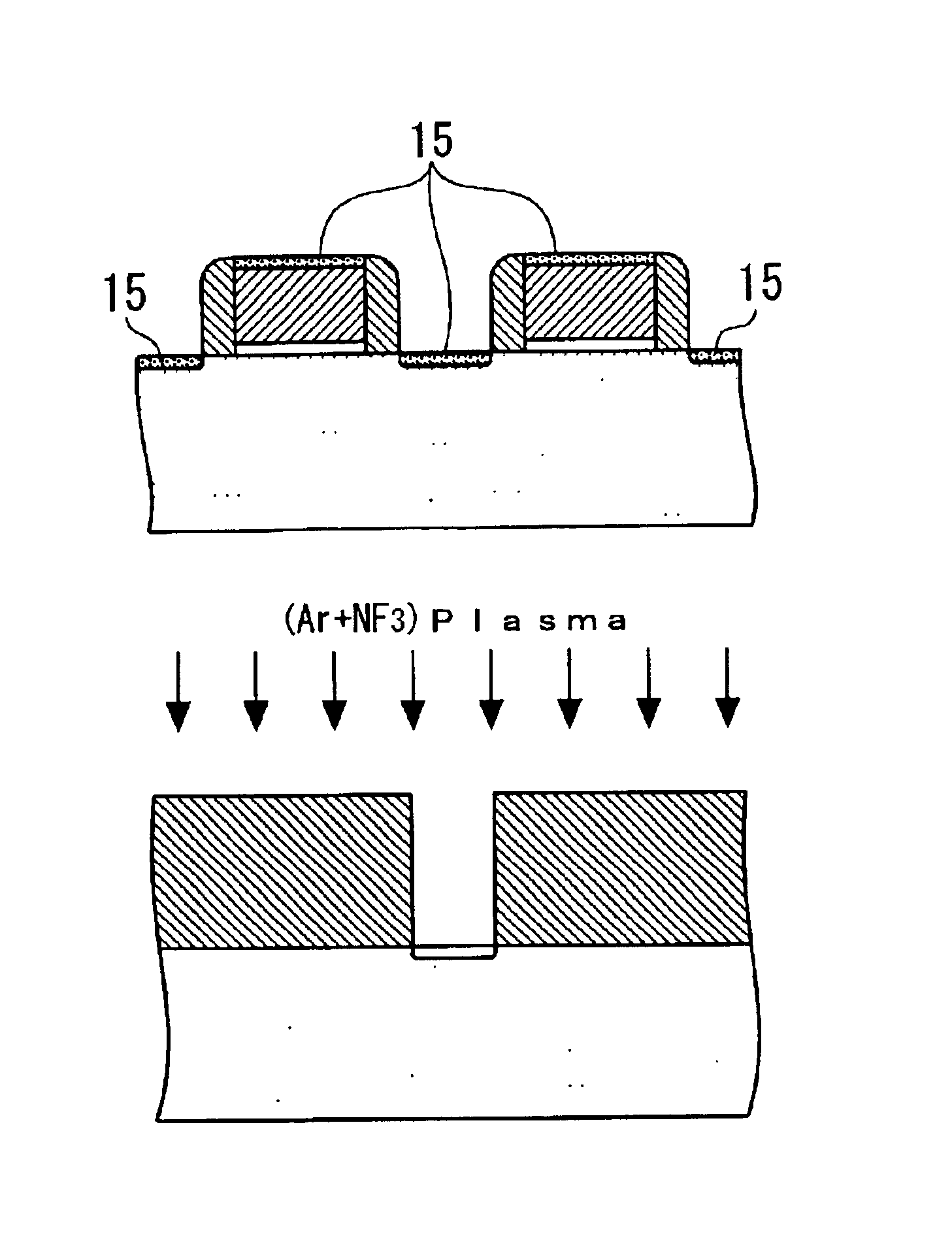
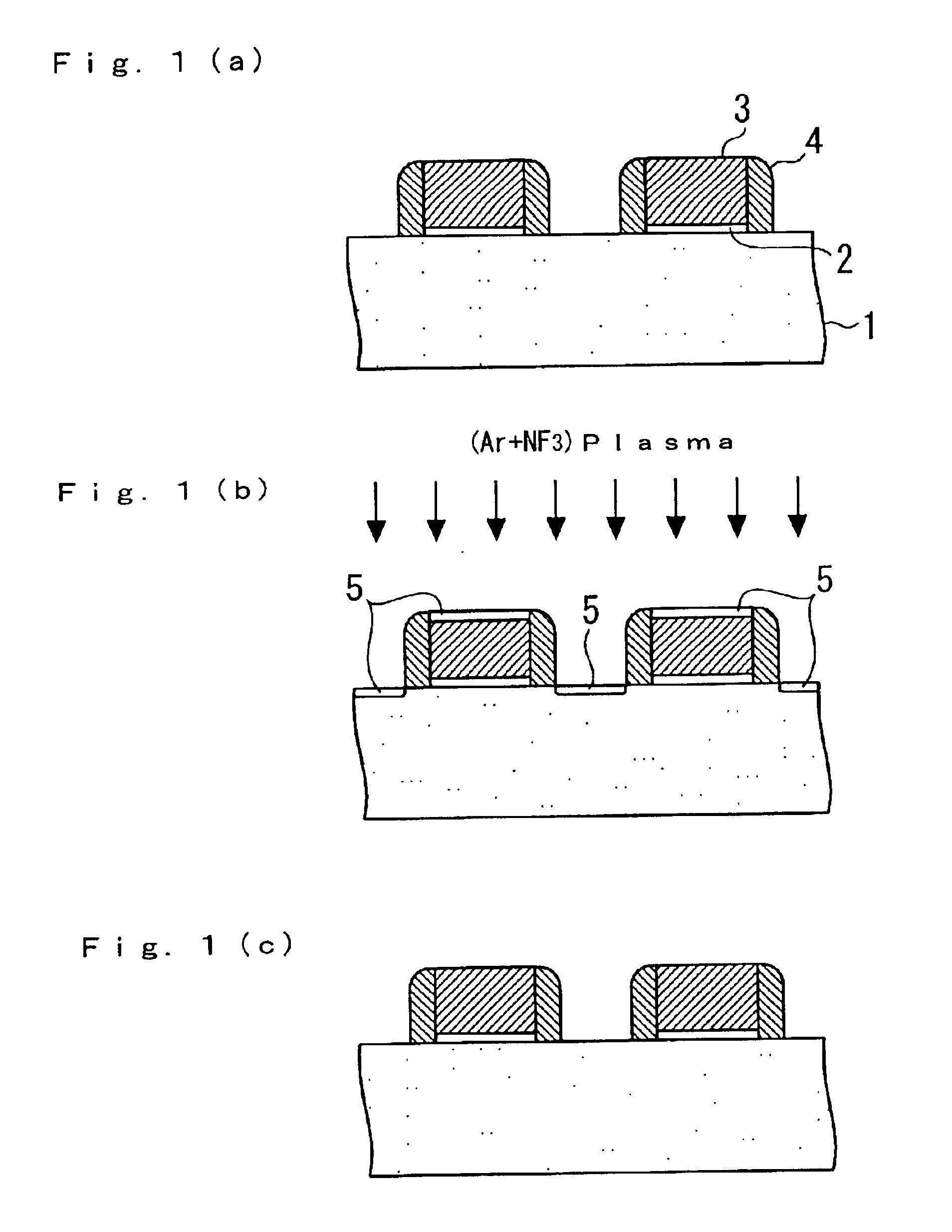
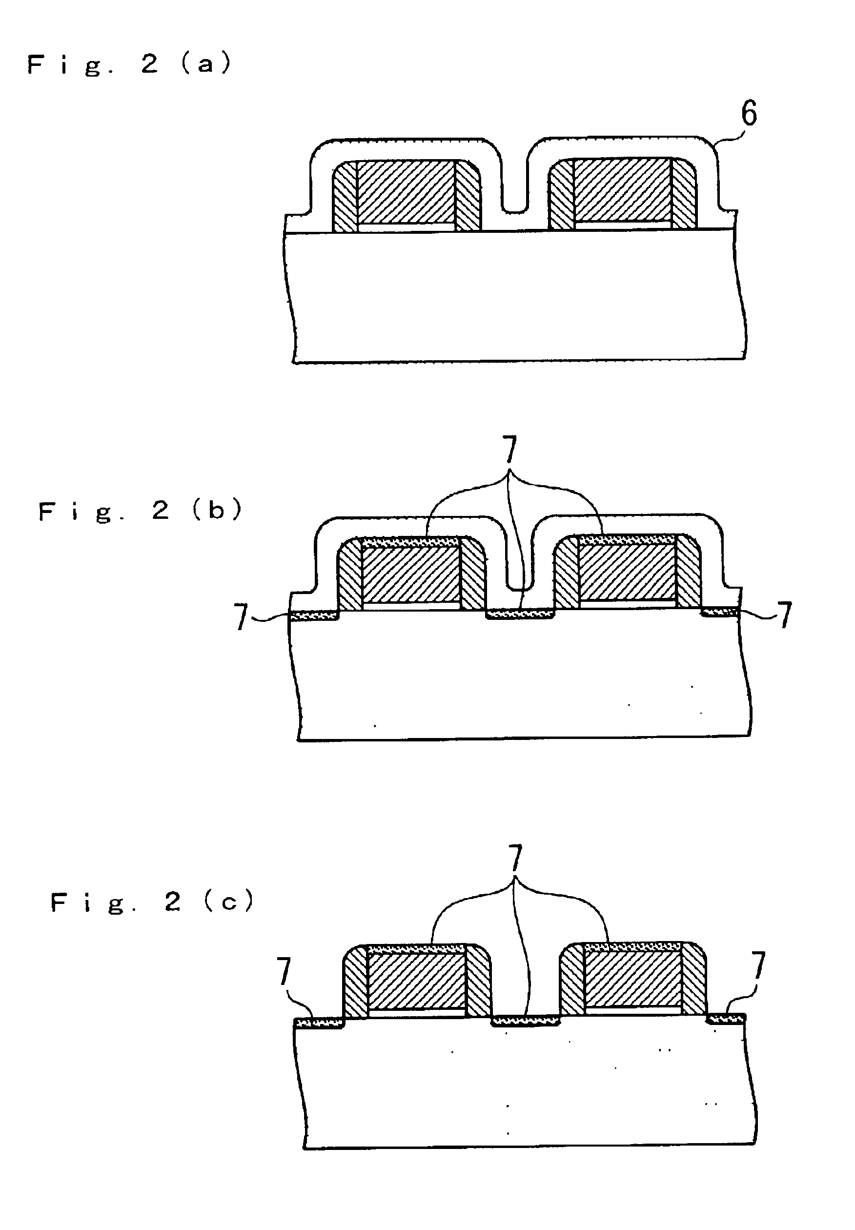
Referring to FIGS. 1 and 2, a method of forming a silicide film according to the embodiment of the invention is described. A gate electrode 3 is formed on a silicon substrate 1 through a gate insulating film 2, after which a side wall 4 made of an insulating film is formed on the side surfaces of the gate electrode 3, respectively, thereby providing a structure of FIG. 1(a). The gate insulating film used may be, for example, a silicon oxide film, a silicon nitride film or the like. Polysilicon may be used as the gate electrode. Moreover, use may be made, as the sidewall, of a silicon oxide film, a silicon nitride film or the like, for example. The sidewall may have a multi-layered structure using a combination of a silicon oxide film and a silicon nitride film. It will be noted that although not particularly shown in FIGS. 1 and 2, the silicon substrate 1 has a source / drain region formed therein by ion implantation.
Initially, the silicon substrate 1 is subjected to RCA washing by us...
second embodiment
Like the first embodiment, agate electrode is formed on a silicon substrate through a gate insulating film, after which a sidewall, made of an insulating film, is formed on the side surfaces of the gate electrode. A silicon oxide film, a silicon nitride film or the like may be used, for example, as the gate insulating film. Polysilicon may be used as the gate electrode. Moreover, a silicon oxide film, a silicon nitride film or the like may be used, for example, as the sidewall. The sidewall may have a multilayered structure using a combination of a silicon oxide film and a silicon nitride film. In addition, a source / drain region may be formed in the silicon substrate by ion implantation.
Initially, the silicon substrate 1 is subjected to RCA washing with a chemical solution based on hydrochloric acid, ammonium hydroxide or the like, thereby removing not only metallic impurities and ionic impurities, but also particulate impurities, all attached to the silicon substrate 1. Subsequentl...
third embodiment
With reference to FIGS. 3 and 4, a method for forming a silicide film according to the invention is described. After a gate electrode 10 is formed on a silicon substrate through a gate insulating film 9, a sidewall 11, made of an insulating film, is formed on the side surfaces of the gate electrode 10 to provide a structure of FIG. 3(a). The gate insulating film used may be made, for example, of a silicon oxide film, a silicon nitride film or the like. Polysilicon may be used as the gate electrode. Moreover, the sidewall used may be made, for example, of a silicon oxide film, a silicon nitride film or the like. The sidewall may have a multi-layered structure made of a combination of a silicon oxide film and a silicon nitride film. Although not particularly shown in FIGS. 3 and 4, a source / drain region is formed within the silicon substrate 8 by ion implantation.
Initially, the silicon substrate 8 is subjected to RCA washing by use of a chemical solution based on hydrochloric acid, am...
PUM
 Abstract
Description
Claims
Application Information