CVD organic polymer film for advanced gate patterning

Inactive Publication Date: 2005-03-08
GLOBALFOUNDRIES INC
View PDF4 Cites 30 Cited by
  • Summary
  • Abstract
  • Description
  • Claims
  • Application Information

AI Technical Summary

Benefits of technology

Embodiments of the invention address the aforementioned problems by substituting an organic polymer layer for the amorphous carbon layer of the bi-layer structure of FIG. 1. In preferred embodiments, the organic polymer layer comprises an organic polymer selected to have substantially no nitrogen. Thus, there is reduced nitrogen contamination of the photoresist via pinholes in the SiON layer. In addition, the organic polymer is selected to have a small or zero compressive stress. Thus, deformation of the organic polymer layer will be reduced. This will result in a reductio

Problems solved by technology

This imposes correspondingly high demands on photolithographic techniques.
However, when a highly reflective substrate such as metal or polysilicon underlies the photoresist layer, reflected light may degrade pattern resolution through several mechanisms.
These include off-normal incident light that is reflected into that is intended to be masked, incident light reflected off device features that exposes “notches” in the photoresist, and thin film interference effects leading to linewidth variations when photoresist thickness changes are caused by irregular wafer topography.
It has been found that some line width variations are due to the inability of the ARC to sufficiently reduce reflective layer reflectivity.
However, the thickness of SiON required for good hardmask performance is too thick to minimize reflectivity.
This thickness may produce non-uniform line width through lensing effects resulting from variations in the topography of reflective layers under the BARC that are not completely phase cancelled by the BARC.
However, there are also accompanying disadvantages of the double layer type anti-reflective layer structure shown in FIG.
One is that thin nitride layers such as SiON layer 108 are prone to pinhole defects that may affect the reliability of the semiconductor device.
One common cause of pinhole defects in a SiON layer is outgassing during the chemical vapor deposition (CVD) process used

Method used


Image

  • CVD organic polymer film for advanced gate patterning
  • CVD organic polymer film for advanced gate patterning
  • CVD organic polymer film for advanced gate patterning

Examples


Embodiment Construction

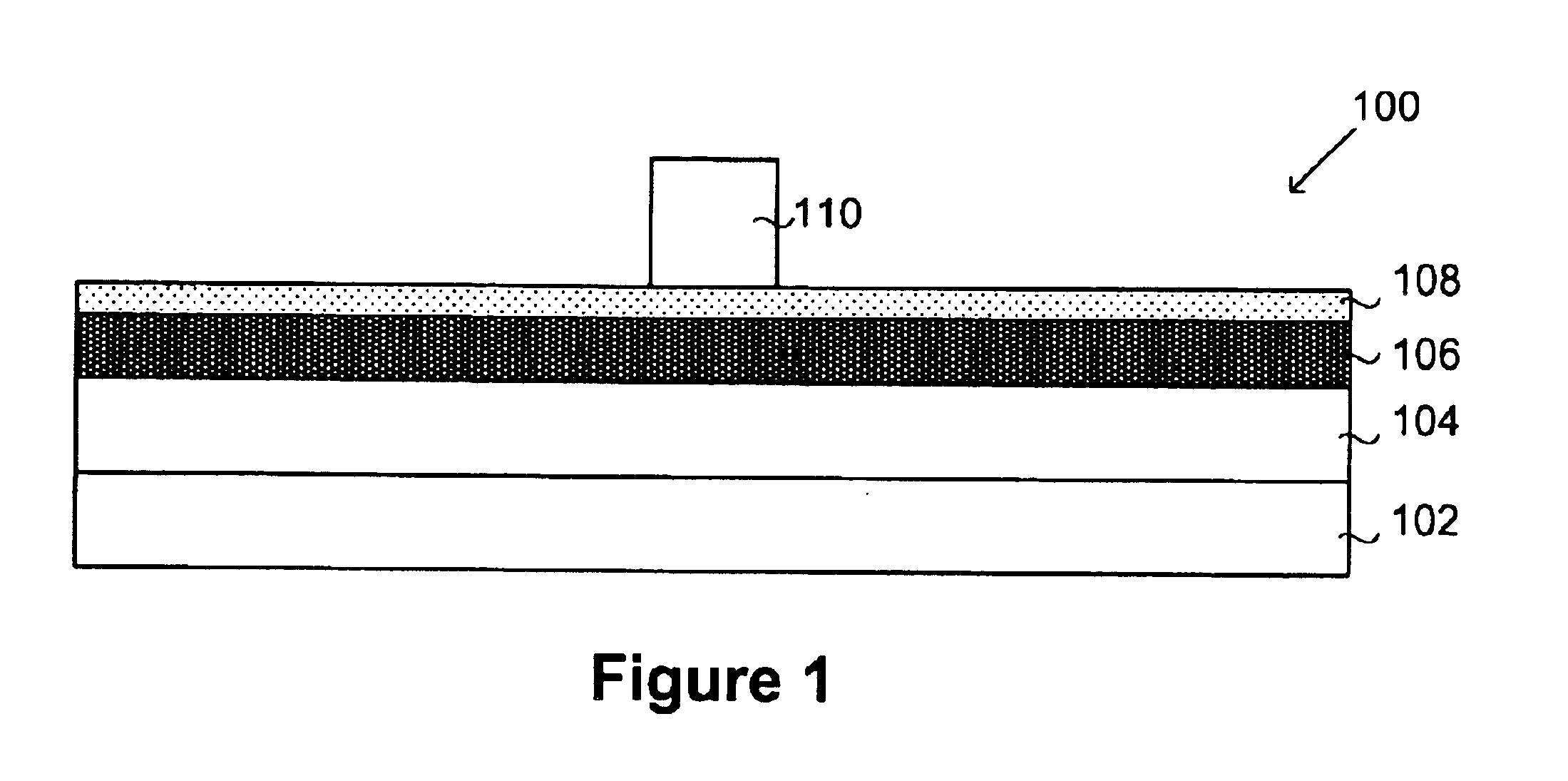
In the following description of preferred embodiments, reference is made to the accompanying drawings which form a part hereof, and in which are shown by way of illustration specific embodiments in which the invention may be practiced. It is to be understood that other embodiments may be utilized and structural changes may be made without departing from the scope of the invention.

As will be apparent to one of ordinary skill in the art, the processes and structures described below do not necessarily form a complete process flow for manufacturing such devices. However, the present invention can be used in conjunction with conventional technology currently employed in the art, for example integrated circuit fabrication methodology, and, consequently, only so much of the commonly practiced processes are included here as are necessary for an understanding of the present invention. As employed throughout the disclosure and claims, the term “substrate” includes, for example, a semiconducto...


PUM


Abstract

A bottom anti-reflective coating comprising an organic polymer layer having substantially no nitrogen and a low compressive stress in relation to a polysilicon layer is employed as the lower layer of a bi-layer antireflective coating/hardmask structure to reduce deformation of a pattern to be formed in a patternable layer. The organic polymer layer is substantially transparent to visible radiation, enabling better detection of alignment marks during a semiconductor device fabrication process and improving overlay accuracy. The organic polymer layer provides excellent step coverage and may be advantageously used in the fabrication of structures such as FinFETs.

Description

BACKGROUND OF THE INVENTION1. Field of the InventionThe present invention pertains integrated circuit fabrication and, in preferred embodiments, to a bottom anti-reflective coating and hard mask for gate patterning and a method for forming the same.2. Related ArtThe escalating requirements for high density and performance associated with ultra large scale integration require responsive changes in conductive patterns, which is considered one of the most demanding aspects of ultra large scale integration technology. High density wiring demands require increasingly denser arrays with minimal spacing between conductive lines. This imposes correspondingly high demands on photolithographic techniques.Photolithographic techniques form patterns in a photoresist layer using a projected light pattern. However, when a highly reflective substrate such as metal or polysilicon underlies the photoresist layer, reflected light may degrade pattern resolution through several mechanisms. These include...

Claims


Application Information

Patent Timeline
IPC IPC(8): H01L21/47H01L21/02H01L31/0232G03F7/09H01L21/033H01L21/28H01L21/3213
CPCG03F7/091H01L21/0332H01L21/32139H01L21/28123H01L29/785
Inventor YOU, LUPLAT, MARINA V.YANG, CHIH YUHBELL, SCOTT A.HUANG, RICHARD J.LYONS, CHRISTOPHER F.CHANG, MARK S.WRIGHT, MARILYN I.
Owner GLOBALFOUNDRIES INC
Why Eureka
Try Eureka