Word line selector for a semiconductor memory

Inactive Publication Date: 2005-03-08
MICRON TECH INC
View PDF9 Cites 22 Cited by
  • Summary
  • Abstract
  • Description
  • Claims
  • Application Information

AI Technical Summary

Benefits of technology

By providing separate doped semiconductor well structures for different groups of word line drivers, the electric potentials applied to word lines belonging to different word line groups can be completely uncorrelated. In particular, in an erase operation, the word lines bel

Problems solved by technology

The global character of the erase operation is a significant disadvantage of conventional flash memories.
This limits the otherwise highly desirable use of flash memories in those applications that require frequent modification of single data bytes o

Method used


Image

  • Word line selector for a semiconductor memory
  • Word line selector for a semiconductor memory
  • Word line selector for a semiconductor memory

Examples


Embodiment Construction

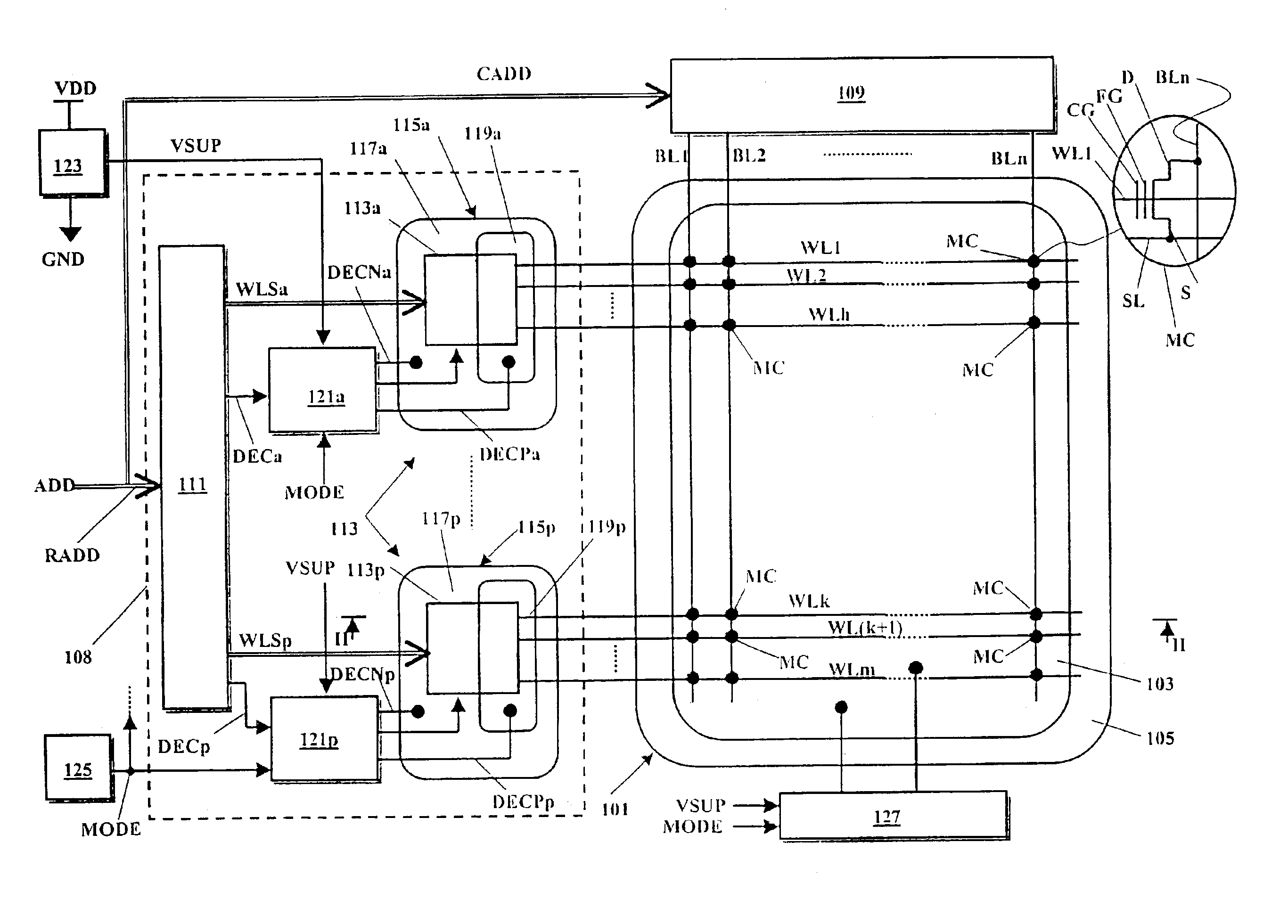
With reference to the drawings, FIG. 1 schematically shows a memory with a word line selector according to an embodiment of the present invention. The memory comprises a two-dimensional array 101 of memory cells MC (depicted for simplicity as dots) arranged by rows (word lines) WL1, WL2, . . . , WLh, . . . , WLk, WL(k+1), . . . , WLm and columns (bit lines) BL1, BL2, . . . , BLn.

The memory cells MC are conventionally formed by stacked-gate MOS transistors with a control gate CG connected to the respective word line, an electrically insulated floating gate FG, a drain D connected to the respective bit line, and a source S connected to a source line common to all the memory cells of the array 101.

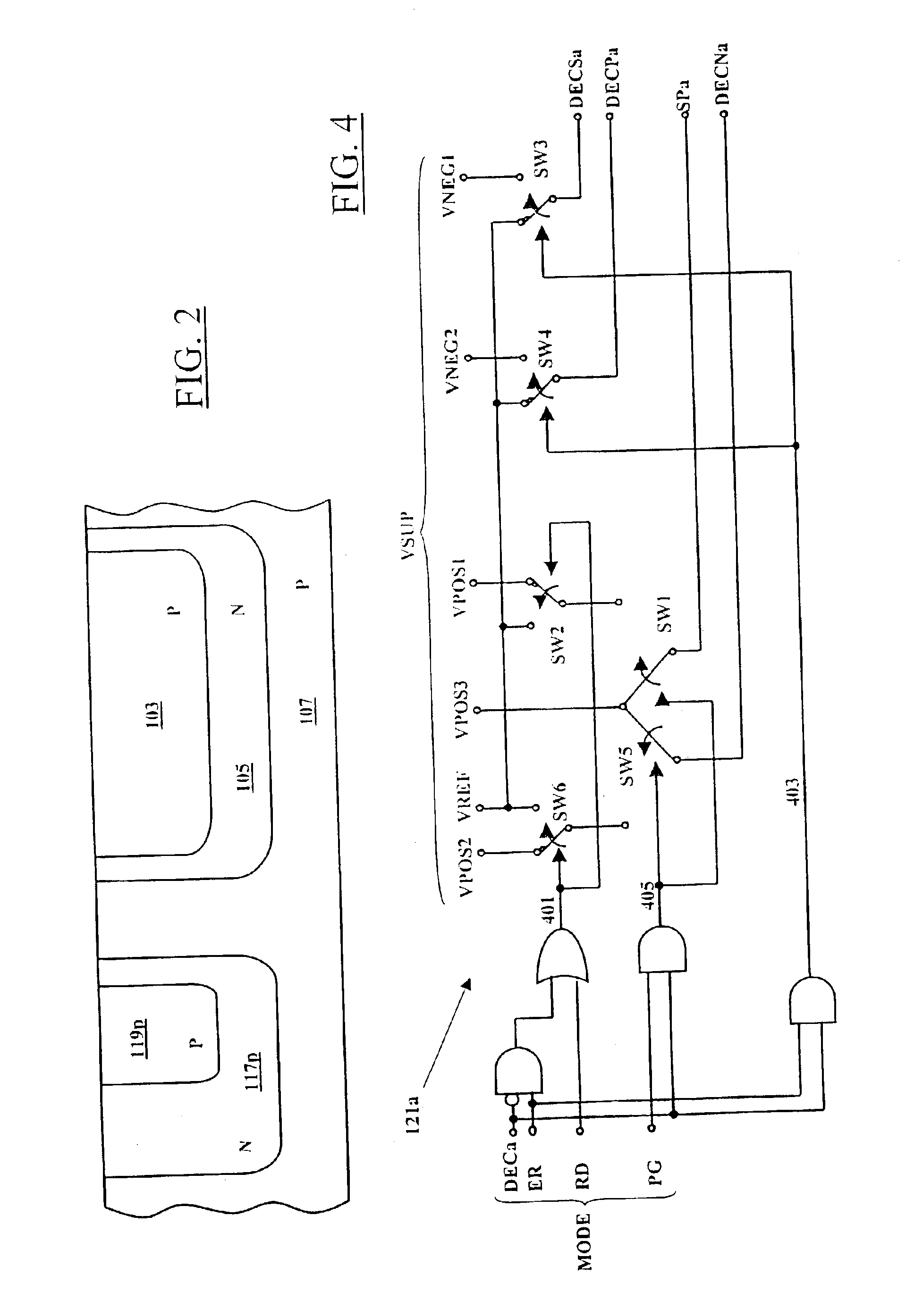
Referring jointly to FIGS. 1 and 2, the memory cells MC are formed within a semiconductor well 103 of a first conductivity type, for example of the P-type for N-channel memory cells; the first-conductivity-type semiconductor well 103 is formed within a semiconductor well 105 of a second condu...


PUM


Abstract

A word line selector for selecting word lines of an array of semiconductor memory cells formed in a doped semiconductor region of a semiconductor substrate comprises a plurality of word line drivers responsive to word line selection signals. Each word line driver is associated with a respective word line for driving the word line to prescribed word line electric potentials, depending on an operation to be conducted on the array of memory cells, in accordance with the word line selection signal.

Description

PRIORITY CLAIMThis application claims priority from European patent application No. 02425084.7, filed Feb. 20, 2002, which is incorporated herein by reference.TECHNICAL FIELDThe present invention relates generally to the field of semiconductor memories, particularly non-volatile memories. More particularly, the invention relates to electrically erasable and programmable non-volatile memories, such as flash memories.BACKGROUND OF THE INVENTIONAs known, data is written (programmed) to a flash memory by means of hot-electron injection into floating-gate electrodes (hereinafter, floating gates) of the memory cells. To erase the data, electrons are extracted from the floating gates of the memory cells by means of the mechanism known as Fowler-Nordheim tunnelling at high electric fields, giving rise to a Fowler-Nordheim current.In conventional flash memories, the erase operation has a global character, affecting the whole array (also called matrix) of memory cells or, where memory sectors...

Claims


Application Information

Patent Timeline
IPC IPC(8): G11C16/16G11C8/10G11C8/00G11C8/08G11C16/08G11C16/06
CPCG11C8/08G11C16/16G11C16/08G11C8/10
Inventor PIO, FEDERICO
Owner MICRON TECH INC
Why Eureka
Try Eureka