Plasma display panel

a technology of display panel and rib wall, which is applied in the direction of gas exhaustion means, instruments, electric discharge tubes, etc., can solve the problems of difficult to make the rib wall equal height, lower production rate, and higher manufacturing cost, and achieve high brightness, high space ratio, and high resolution

Inactive Publication Date: 2005-03-15
NANJING HUAXIAN HIGH TECH CO LTD
View PDF8 Cites 8 Cited by
  • Summary
  • Abstract
  • Description
  • Claims
  • Application Information

AI Technical Summary

Benefits of technology

An object of present invention is to provide a plasma display panel (PDP), in which, a conductive plate with array of meshes is used as common electrodes, group of orthogonal electrodes are used as addressing and scanning electrodes which can provide high resolution, high brightness, high space ratio and lower working voltage as well as high production rates and low cost.

Problems solved by technology

Secondly, a voltage is applied between the scanning electrodes and the common electrodes to form a glow discharge.
Firstly, it is difficult to make the rib walls with equal height, equal width while keeping narrow size in large size with dielectric materials.
This causes lower production rate, so does to higher manufacture cost.
Secondly, because of the width of scanning electrodes and common electrodes, it is difficult to make fine pixels along the horizontal direction and improve the definition.
Lastly, the drive circuits is complicate with high cost and power consuming because the addressing discharge space are formed by separating the substrates using the high precision rib walls and it is difficult to achieve uniformity for the whole panel.

Method used


Image

  • Plasma display panel
  • Plasma display panel
  • Plasma display panel

Examples


example 1

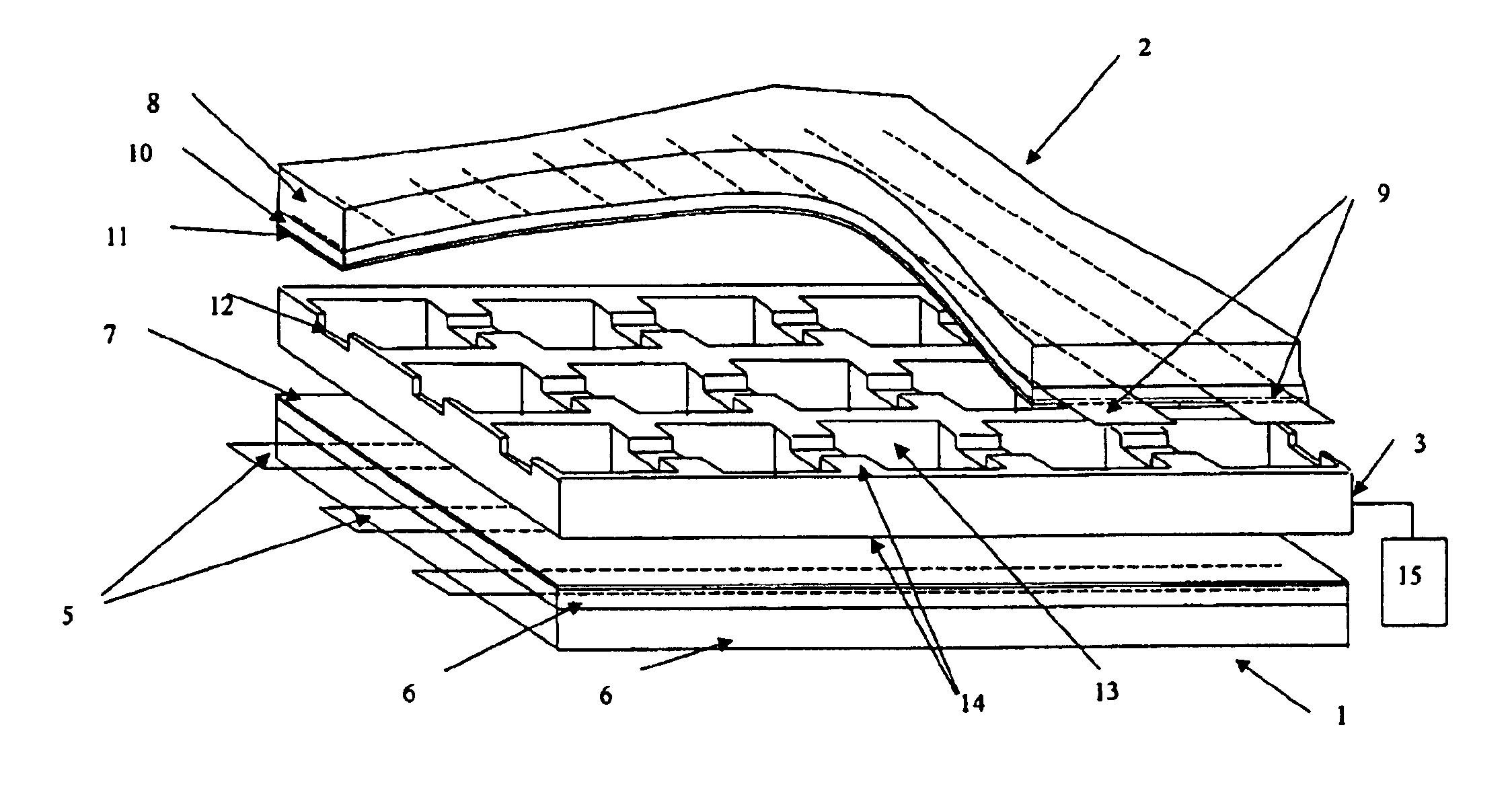
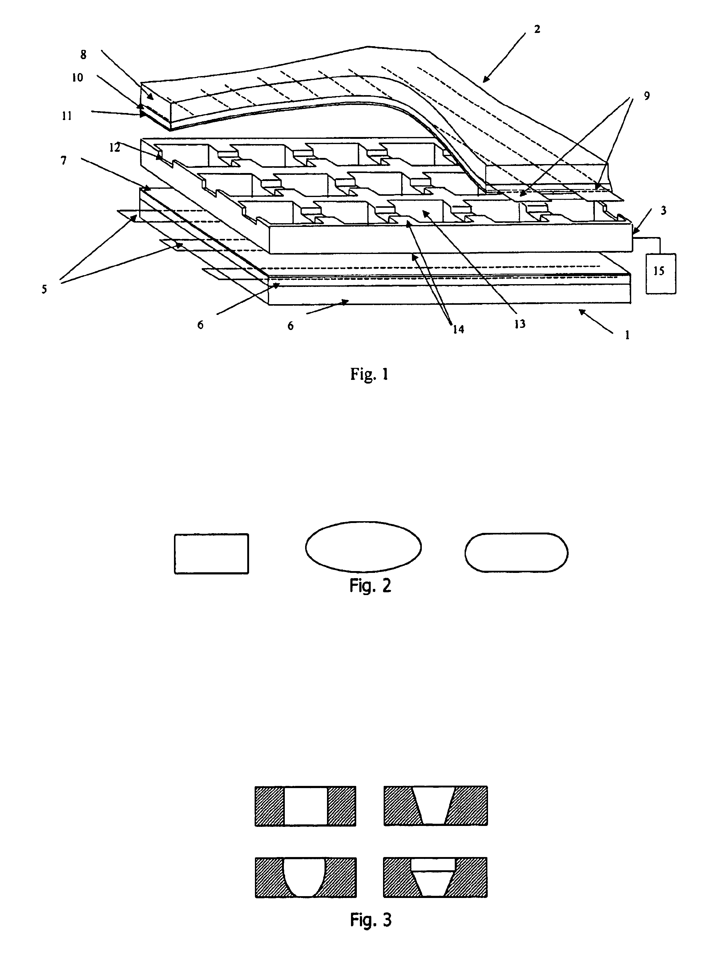
The first example of this invention includes a rear substrate 1, a front substrate 2 and a conductive plate with meshes 3 as shown in FIG. 1, said rear substrate 1 comprises a rear glass plate 4, first electrodes 5 formed on said rear glass plate 4, a dielectric layer 6 formed on said rear glass 4 embedding said first electrodes 5 and a protecting film 7 coated on said dielectric layer; said front substrate 2 comprises a front glass plate 8, second electrodes 9 formed on the bottom surface of said front glass plate 8 which is transparent and orthogonal to said first electrodes 5, a dielectric layer 10 formed on the surface of said front glass plate 8 embedding said second electrodes 9 and a protective film 11 coated on said dielectric layer 10; said conductive plate with meshes 3 located between said rear substrate 1 and front substrate 2. The conductive plate 3 is made of conductive materials with array of meshes. Each mesh is perpendicular to said first electrode 5 and second elec...

example 2

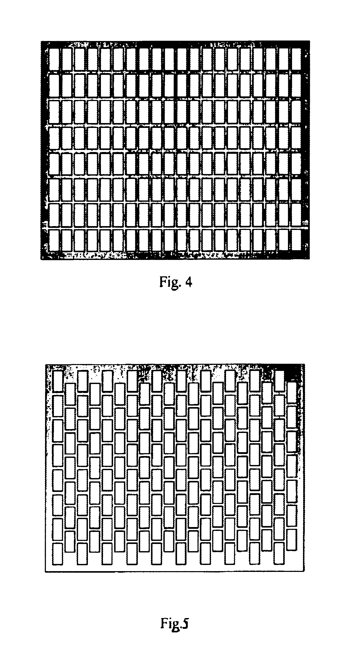
In present example, the shape of the meshes in said conductive plate 3 described in Example 1 can be squares, polygon (including rectangle), ellipse (including circle) etc. as well as the combination of various shapes as shown in FIG. 2. The sectional structure can be rectangle, trapezoid, ellipse arc (including circle arc) etc. as well as the combination of various shapes as shown in FIG. 3. The distribution of said meshes can be parallel arrangement or alternate arrangement. It can be equidistance arrangement or un-equidistance arrangement. It can also be random arrangement.

example 3

In present example, one of the three electrodes, i.e. said conductive plate with array of meshes 3, said first electrodes 5 and said second electrodes 9, is covered by dielectric layer while other electrodes, which are made of anti-ion-bombard conductive material or covered by protective film, are exposed to the working gas; or two of the three electrodes, i.e. said conductive plate with array of meshes 3, said first electrodes 5 and said second electrodes 9, except that said first electrodes 5 and second electrodes 9 are covered by dielectric layer as described in Example 1, are covered by dielectric layer while other electrode, which is made of anti-ion-bombard conductive material or covered by protective film, is exposed to the working gas; or all of the three electrodes, i.e. said conductive plate with array of meshes 3, said first electrodes 5 and said second electrodes 9, are covered by dielectric layer.


PUM


Abstract

The plasma display panel of present invention comprises a front plate, a rear plate and a conductive mesh plate sandwiched between said front plate and said rear plate for supporting them. Said mesh plate includes an array of mashes which, together with the addressing electrode on said rear plate and the scanning electrode on said front plate, form the discharge cell of the display panel. Said mesh plate has gas conductive grooves on its surface in the region between adjacent mashes. The present invention has the advantage of higher resolution, brightness, and light transmissivity as well as lower operating voltage compared with those of the plasma display panel in prior art. In addition, the present invention provides high rate of finished products and low manufacturing cost.

Description

FIELD OF THE INVENTIONThe present invention relates to a plasma display panel, in particularly, to coplanar plasma display panel.DESCRIPTION OF THE PRIOR ARTA conventional three electrodes surface discharge AC PDP comprises a front substrate and a rear substrate. The rear substrate includes a underlay glass plate, addressing electrodes on the surface of said underlay glass plate, a dielectric layer on the surface of said underlay glass plate embedding the addressing electrodes, rib walls on the dielectric layer made of dielectric materials to keep a discharge distance and prevent from disturb discharge. The front substrate comprises a glass plate for assembling with said rear substrate, common electrodes and transparent scanning electrodes alternately on the bottom surface of the glass plate in a striped pattern being perpendicular to said addressing electrodes, a dielectric layer formed on the bottom surface of the front glass plate including common and transparent scanning electro...

Claims


Application Information

Patent Timeline
Patent Type & Authority Patents(United States)
IPC IPC(8): H01J17/49H01J11/02H01J11/12H01J11/36
CPCH01J11/36H01J11/12H01J11/20H01J11/54
Inventor ZHANG, XIONGWANG, BAO-PING
Owner NANJING HUAXIAN HIGH TECH CO LTD
Why Eureka
Try Eureka