Off-center solder ball attach assembly

a solder ball and assembly technology, applied in the direction of printed circuit parts, lithographic masks, non-printed masks, etc., can solve the problems of reducing the reliability of the connection component, poor bonding between the molten solder and the contact pad, and adverse effects of solder ball oxidation on the ability of the solder ball to wet to and ultimately bond with the contact pad

Inactive Publication Date: 2005-03-22
TESSERA INC
View PDF21 Cites 18 Cited by
  • Summary
  • Abstract
  • Description
  • Claims
  • Application Information

AI Technical Summary

Benefits of technology

In certain preferred embodiments, the first conductive elements are conductive pads and the second conductive elements are conductive traces having tip ends releasably secured to the dielectric element. The vias preferably extend between the first and second surfaces of the dielectric element. Each via preferably has an open end adjacent the first surface of the dielectric element. In certain preferred embodiments, one or more vias may have a closed end adjacent the second surface of the dielectric element. The method preferably includes positioning solder balls atop one or more of the first conductive elements, and reflowing the solder balls for permanently attaching the solder balls to the first conductive elements. The solder balls may be positioned by first depositing a pad of a flux material atop each first conductive element and then placing a solder ball atop each flux pad. In other embodiments, the solder balls may be positioned by providing a stencil having a plurality of openings, juxtaposing the stencil with the first surface of the dielectric element so that the stencil openings are in substantial registration with the first conductive elements, and placing a solder ball in each stencil opening so that a solder ball is positioned atop each first conductive elements. The stencil is desirably maintained in juxtaposition with the first surface of the dielectric element during the reflowing step.
At the commencement of the reflowing step, at least a portion of one or more via openings are exposed. In other words, after the solder balls have been positioned atop the conductive pads and at the beginning of the reflowing step, the solder balls will not completely cover the via openings. As a result, when the solder balls are heated up during reflow, the expanding air and / or flux vapors in the vias can escape through the via openings before the openings are completely covered by molten solder material.

Problems solved by technology

The presence of oxides on solder balls adversely affects the ability of the solder balls to wet to and ultimately bond with contact pads.
As is well known to those skilled in the art, if an oxide layer is not adequately removed from a contact pad, then molten solder will not wet to the pad, thereby resulting in the formation of a poor bond between the molten solder and the contact pad.
As mentioned above, the voids may dramatically diminish the reliability of the connection component.
This is because the solder balls with voids have a tendency to crack during thermal cycling which may adversely affect the ability of the connection component to maintain an electrical interconnection with another circuit element.
Moreover, the existence of voids in solder balls may cause the solder balls to be improperly dimensioned.
Such improperly dimensioned solder balls will cause non-planarity of a package, making it difficult to place the package in a test socket or attach the package to a substrate.
As a result, packages having improperly dimensioned solder balls with voids are rejected at a much higher rate than packages having properly dimensioned solder balls.

Method used


Image

  • Off-center solder ball attach assembly
  • Off-center solder ball attach assembly
  • Off-center solder ball attach assembly

Examples


Embodiment Construction

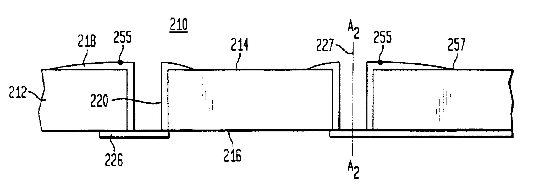
FIGS. 2A-2D shows a preferred method of attaching solder balls to a connection component that minimizes the voiding problems described above. Referring to FIG. 2A, a connection component 110 includes a flexible dielectric layer 112 having a first surface 114 and a second surface 116 remote therefrom. The connection component 110 includes conductive pads 118 atop the first surface 114 and metalized vias 120 that extend between the first surface 114 and the second surface 116 of the dielectric sheet 112. Each via 120 has a center 121 and an open end 123 adjacent the first surface 114 of dielectric layer 112. The center 121 of via 120 shown in FIG. 2A is defined by axis A1—A1. Thus, the center 121 of each via 120 preferably in located along a line that is equidistant from the sidewalls of the via 120. Each via 120 may also include a closed end 125 remote from the open end 123. In the particular embodiment shown in FIG. 2A, the closed end 125 of via 120 is adjacent the second surface 11...


PUM


Abstract

A connection component includes a dielectric element having a first surface and a second surface, and conductive pads on the first surface of the dielectric element, each conductive pad having a center. The connection component also includes conductive vias electrically connected to the conductive pads and extending toward the second surface of the dielectric element, each of the vias having an opening at one of the conductive pads. At least one of the via openings is offset from the center of at least one of the conductive pads.

Description

BACKGROUND OF THE INVENTIONThe present invention relates to microelectronic connection components and more specifically relates to methods of attaching solder balls to conductive pads or terminals on a microelectronic element, such as a microelectronic connection component.Soldered connections are typically used throughout the electronics industry to connect electronic components. Where the components to be connected include dielectric elements, such as a printed circuit board or a flexible dielectric sheet having conductive metal traces, the traces may be provided with enlarged regions, commonly referred to as “lands” or “conductive pads.” A mass of solder may be deposited on each conductive pad by exposing the assembly to a liquid solder or, more typically, by applying solder preforms commonly referred to as “solder balls” onto the pads and heating the assembly to melt or reflow the solder balls. Solder balls are typically reflowed by raising the temperature of the solder balls ab...

Claims


Application Information

Patent Timeline
Patent Type & Authority Patents(United States)
IPC IPC(8): H01L21/02H01L21/48H05K3/34
CPCH01L21/4853H05K3/3478H05K2201/09509H05K2203/1178H05K2203/041H05K2203/043H05K2203/0557H05K2201/0959
Inventor ZOHNI, WAEL
Owner TESSERA INC
Why Eureka
Try Eureka