Symmetrical stacked inductor

a technology of inductors and stacked inductor bodies, which is applied in the direction of inductors, transformers/inductances, transformers/reacts mounting/support/suspension, etc., can solve the problems of large circuit layout area, high cost, and ineffective phase noise reduction, and achieve the effect of decreasing the quantity of inductors

Inactive Publication Date: 2005-03-22
NAT CENT UNIV
View PDF2 Cites 39 Cited by
  • Summary
  • Abstract
  • Description
  • Claims
  • Application Information

AI Technical Summary

Benefits of technology

It is an object of the present invention to provide a symmetrical stacked inductor which discloses a structure mad

Problems solved by technology

The effect of high frequency wireless communication focuses on the design of the radio frequency circuit, and the high frequency inductor of the radio frequency circuit requires a high quality factor(Q), high self-resonant frequency,

Method used


Image

  • Symmetrical stacked inductor
  • Symmetrical stacked inductor
  • Symmetrical stacked inductor

Examples


Embodiment Construction

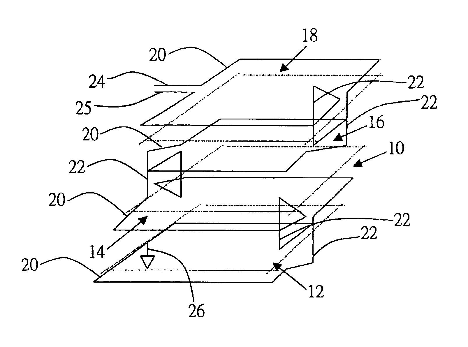
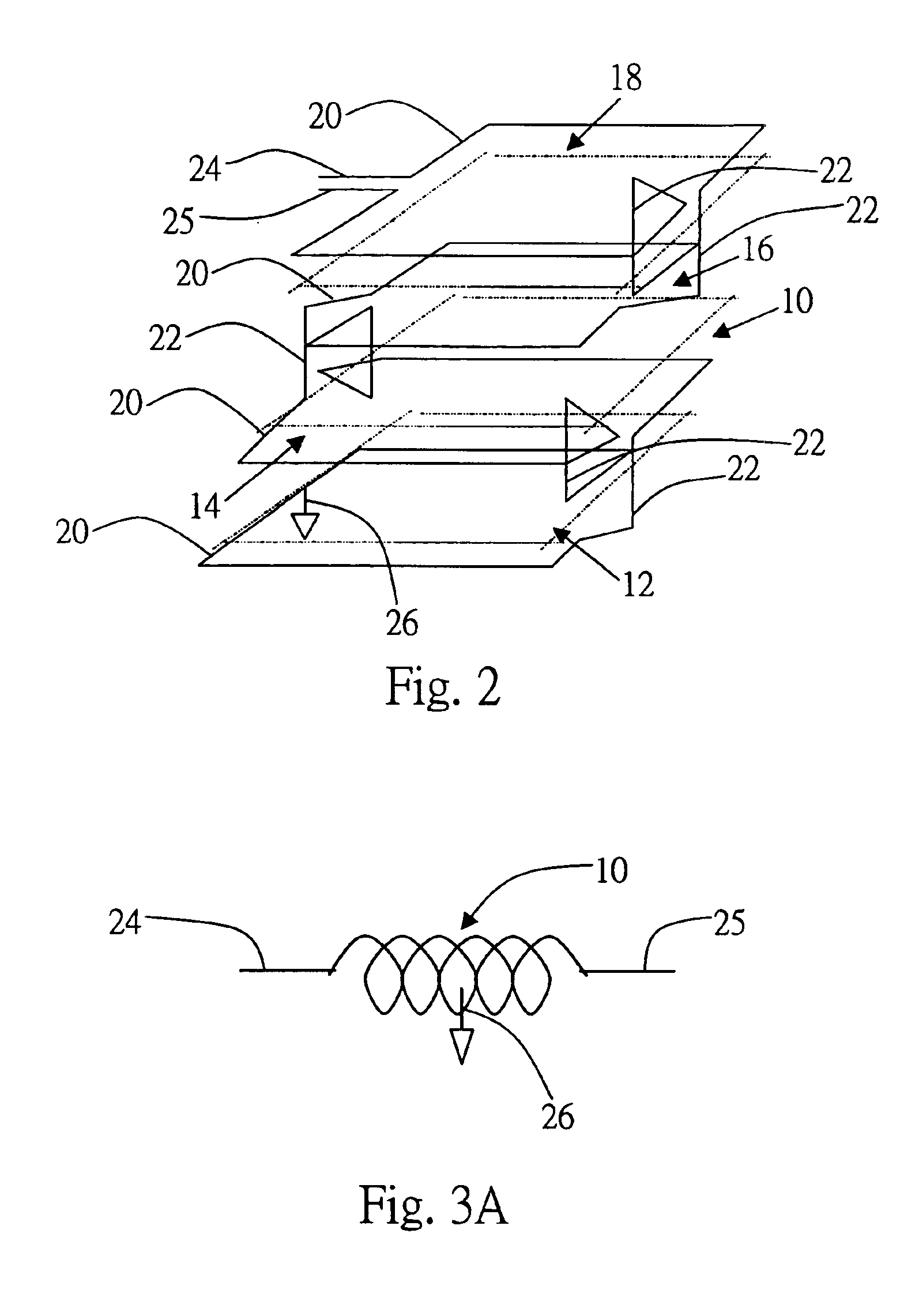
Refer to FIG. 2, an embodiment of the present invention is directed to a symmetrical inductor 10 formed on the semiconductor and it comprises a first conductive layer 12, a second conductive layer 14, a third conductive layer 16 and a fourth conductive layer 18 wherein each conductive layer 12, 14, 16, 18 is a symmetrically and geometrically shaped conductive layer and on a respective plane of the inter-metal dielectric layer of the semiconductor. The conductive layers 12, 14, 16, 18 are isolated respectively by an inter-metal dielectric layer (depicted by dotted lines), and each of them use at least a conductive line 20 forming a symmetrical and geometric conductive layer. Further, the diameters of the even conductive layers 14, 18 (second and fourth layers) and those for the odd conductive layers 12, 16 (first and third layers) can be different to reduce parasitic capacitance. The form of the conductive layers 12, 14, 16, 18 could be, for example, circular or other forms. A plural...


PUM


Abstract

A symmetrical stacked inductor comprising a plurality of conductive layers using at least one conductive line formed out of a symmetrical and geometric conductive layer and having at least one inter-metal dielectric layer for isolating each conductive layer, and wherein the conductive line does not intersect; and a plurality of vias placed between the inter-metal dielectric layers for electrical conduction.

Description

BACKGROUND OF THE INVENTION1. Field of the InventionThe present invention relates to a stacked inductor, more particularity, to a symmetrical stacked inductor made by a semiconductor process and applied to a radio frequency circuit.2. Description of the Related ArtThe rapid development of communication technology forced the communication market to expand and requires more channels. Presently, portable communication devices have developed into devices with high frequency, light, thin, short, small and multiple functions so that the requirement of high accuracy, exactitude, credibility and modularizing is needed. The effect of high frequency wireless communication focuses on the design of the radio frequency circuit, and the high frequency inductor of the radio frequency circuit requires a high quality factor(Q), high self-resonant frequency, low parasitic capacitance output and high stability, but it is hard to observe all factors during design.Refer to FIG. 1, the conventional induc...

Claims


Application Information

Patent Timeline
IPC IPC(8): H01F17/00H01L27/08
CPCH01L27/08H01F17/0013
Inventor CHEN, WEI-ZENCHEN, WEN-HUI
Owner NAT CENT UNIV
Why Eureka
Try Eureka