Power semiconductor module

Active Publication Date: 2005-03-22
SEMIKRON ELECTRONICS GMBH & CO KG
View PDF19 Cites 37 Cited by
  • Summary
  • Abstract
  • Description
  • Claims
  • Application Information

AI Technical Summary

Benefits of technology

An object of the present invention is to provide a power semiconductor module that enables the easy replacement of at least o

Problems solved by technology

Unfortunately, efforts to improve performance capacity, reliability, and life expectancy, while simultaneously decreasing manufacturing costs have been unsuccessful
One disadvantage of the conventional design is that, particularly for large-surface solder joints on heat sinks, it is difficult to predictably control the quality of the solder joint.
Low-quality solder joints and lack of process predictability reduce the reliability and the life expectancy of the resultant power semiconductor modules.
Unfortunately, pressure buildup in pressure-contacted power semiconductor modules is conventionally accomplished by means of a mechanically stable pressure plate.
Unfortunately, the power semiconductor modules shown in DE 196 48 562 C1 and DE 199

Method used


Image

  • Power semiconductor module
  • Power semiconductor module
  • Power semiconductor module

Examples


Example

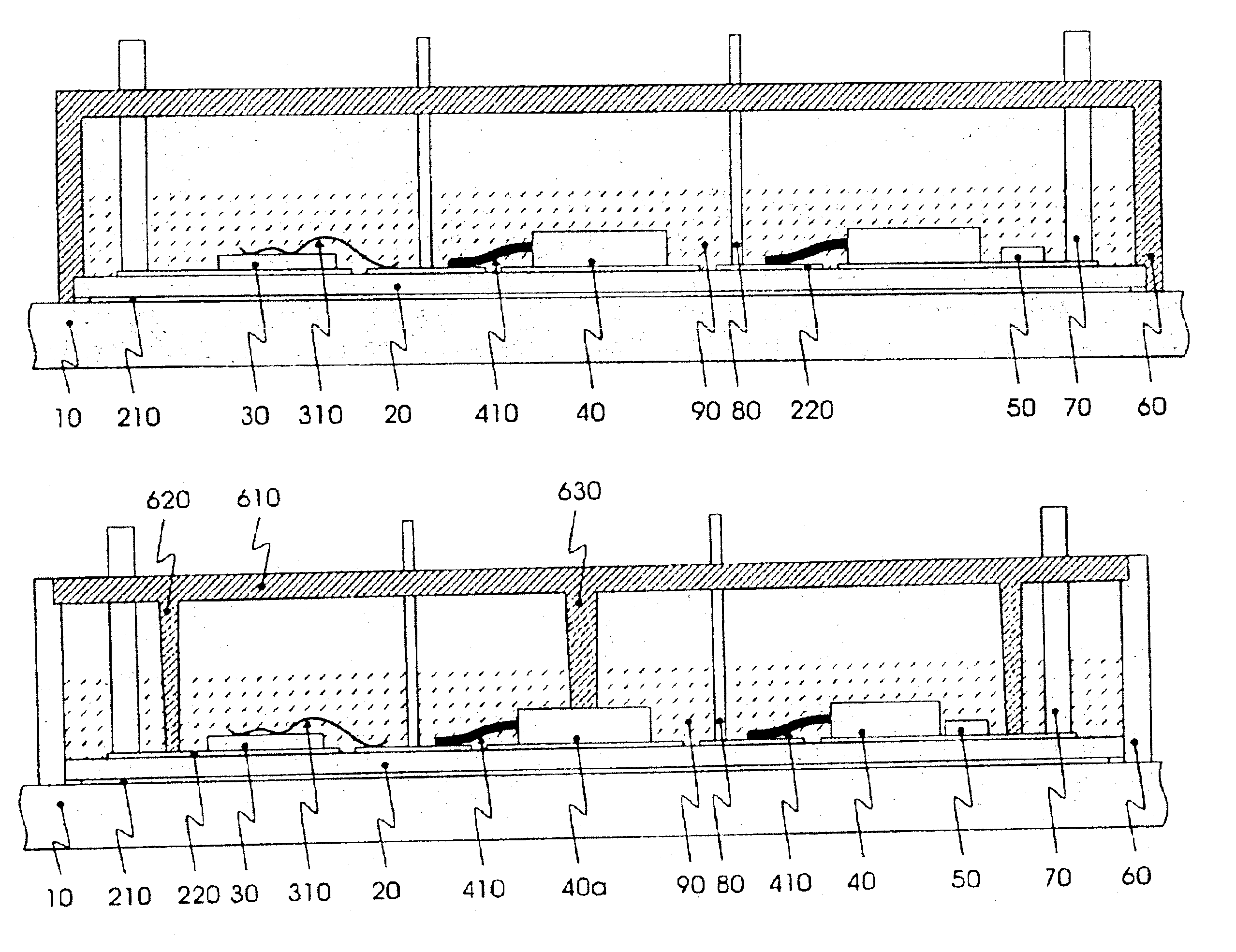
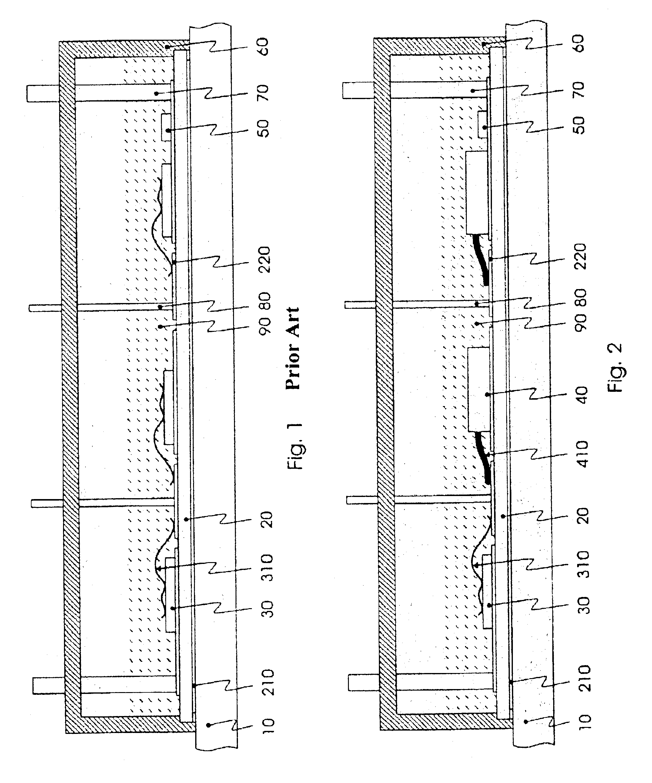
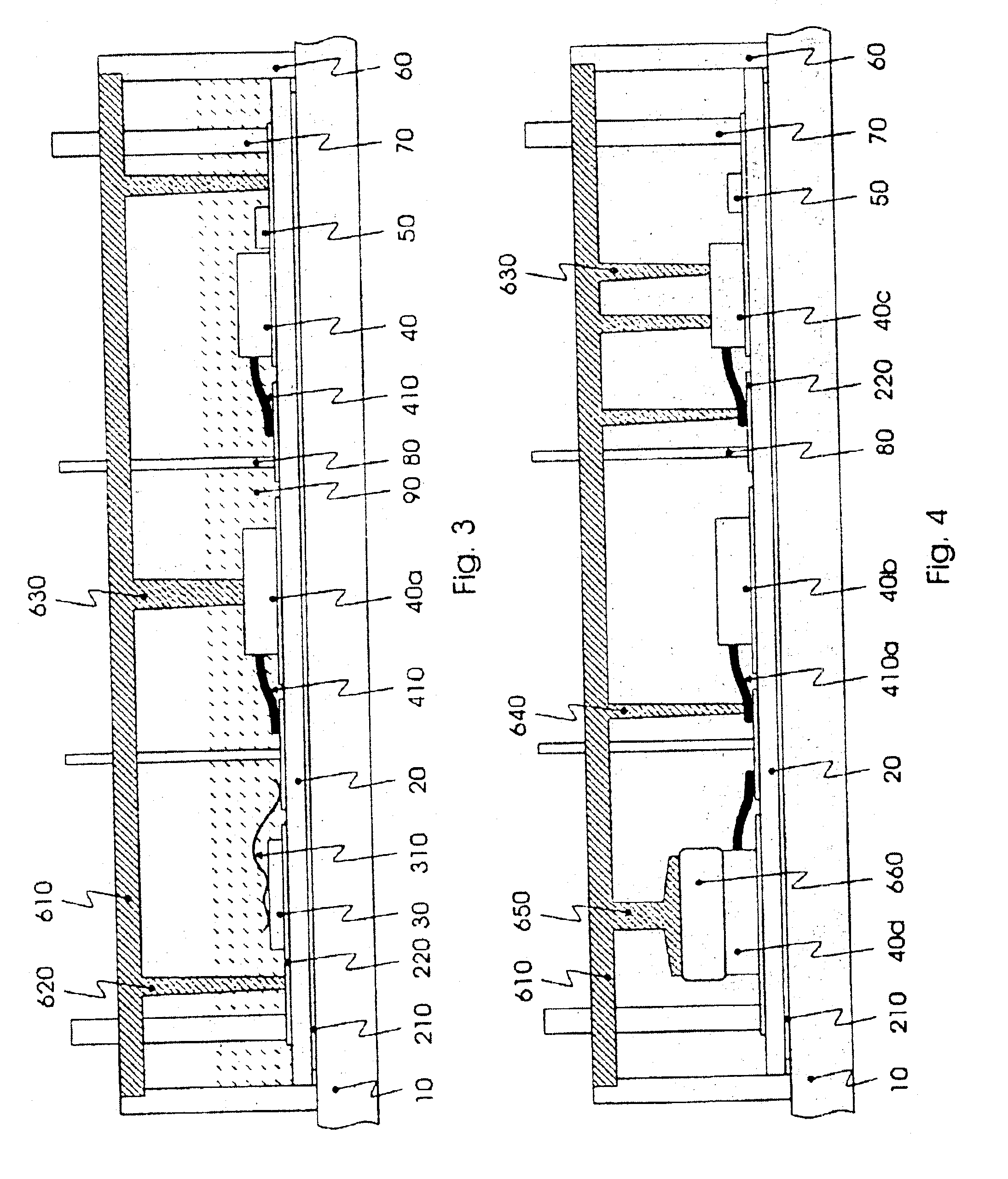
The present invention enables replacement of at least one unhoused (unencapsulated) chip-shaped power semiconductor element with a housed (encapsulated) power semiconductor for improved manufacturing. Further, the housed semiconductor elements have the advantage that they include connecting elements extending from the housing, with which the same electrical contacts can be established as those established in conventional designs by means of wire bondings. Consequently, the present invention may be immediately placed into service with conventional manufacturing practices for substantial benefit. Both, the housed and unhoused power semiconductor elements may be connected with the substrate using conventional soldering or adhesive, but only the present invention provides for assured contact without these traditional bonding techniques.

Referring now to FIG. 2, a power semiconductor module includes a set of housed power semiconductor elements 40 in place of conventional individual chip-s...


PUM


Abstract

The invention provides a power semiconductor module including a power converter module with an improved configuration technology that minimizes or eliminates the need for a positive bonding (soldering/adhesive) connection between a power semiconductor element and a contact surface of a substrate. The present invention includes a housed or encapsulated power semiconductor element with a pre-secured connecting element that reduces manufacturing time and costs, while improving performance capability in a decreased size.

Description

BACKGROUND OF THE INVENTION1. Field of the InventionThe present invention relates to an improved power semiconductor module having active and passive components including a power converter module. More specifically, the present invention relates to a power semiconductor module that includes a housed (encapsulated) power semiconductor element having contact elements and offers substantial manufacturing advantages.2. Description of the Related ArtSeveral power semiconductor modules with active and passive components (including power converter modules) have been described in the literature. Unfortunately, efforts to improve performance capacity, reliability, and life expectancy, while simultaneously decreasing manufacturing costs have been unsuccessfulModern power semiconductor modules, are modules without base plates, as can be seen in, for example DE 199 03 875 A1. This type of modern power semiconductor module includes:(1) an outer housing,(2) a ceramic substrate supporting circuit-...

Claims


Application Information

Patent Timeline
IPC IPC(8): H01L23/48H01L25/03H01L25/11H01L25/10H05K1/03H05K1/18H05K3/32
CPCH01L24/72H01L25/072H01L25/115H05K1/181H01L2924/01033H01L2924/01005H05K2201/10318H05K2201/10166H05K3/325H01L2224/48227H01L2224/4846H01L2224/48472H01L2924/01029H01L2924/01082H01L2924/19043H05K1/0306H05K3/0061H01L2924/00H01L2924/15787Y02P70/50
Inventor GOEBL, CHRISTIAN
Owner SEMIKRON ELECTRONICS GMBH & CO KG
Why Eureka
Try Eureka