
Semiconductor module and power conversion device

Active Publication Date: 2005-03-29
HITACHI ASTEMO LTD
View PDF15 Cites 10 Cited by
  • Summary
  • Abstract
  • Description
  • Claims
  • Application Information

AI Technical Summary

Benefits of technology

The present invention is to provide a semiconductor module that can be improved in cooling performance. The present invention is also to provide a highly reliable, compact, and inexpensive power conversion device that can maintain normal operation even when used under a severe heat-cycle environment.

Problems solved by technology

For the power conversion devices used under a severe heat-cycle environment, such as the power conversion device mounted in an automobile, as the standards pertaining to power supplies are tightened, the magnitude of the current flowing through semiconductor devices increases and this, in turn, increases the heat emitted from the semiconductor devices and makes the heat cycle even severer.

Method used


Image

  • Semiconductor module and power conversion device
  • Semiconductor module and power conversion device
  • Semiconductor module and power conversion device

Examples


first embodiment

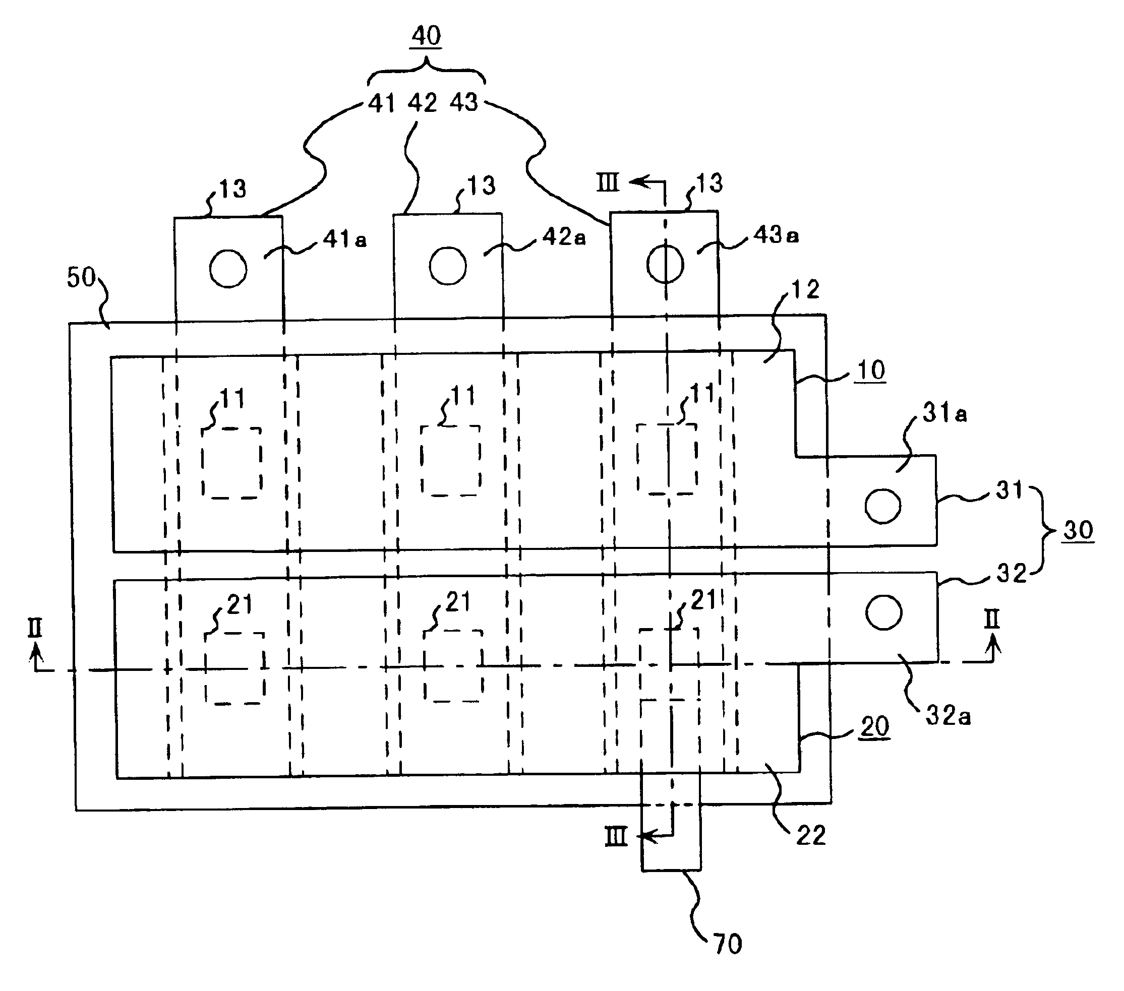
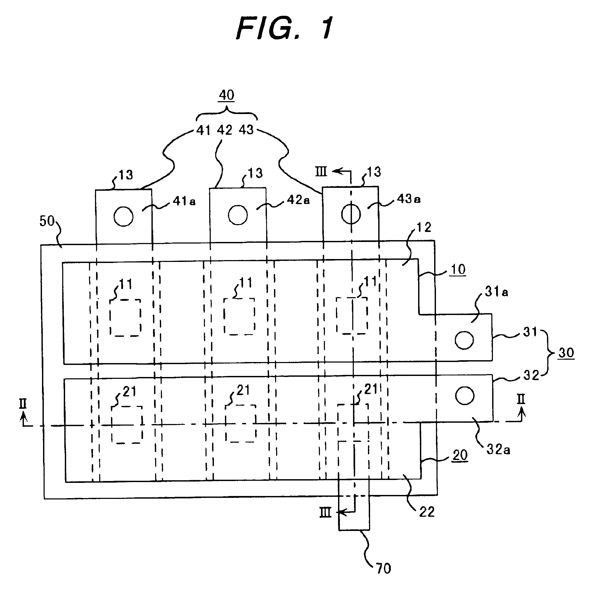
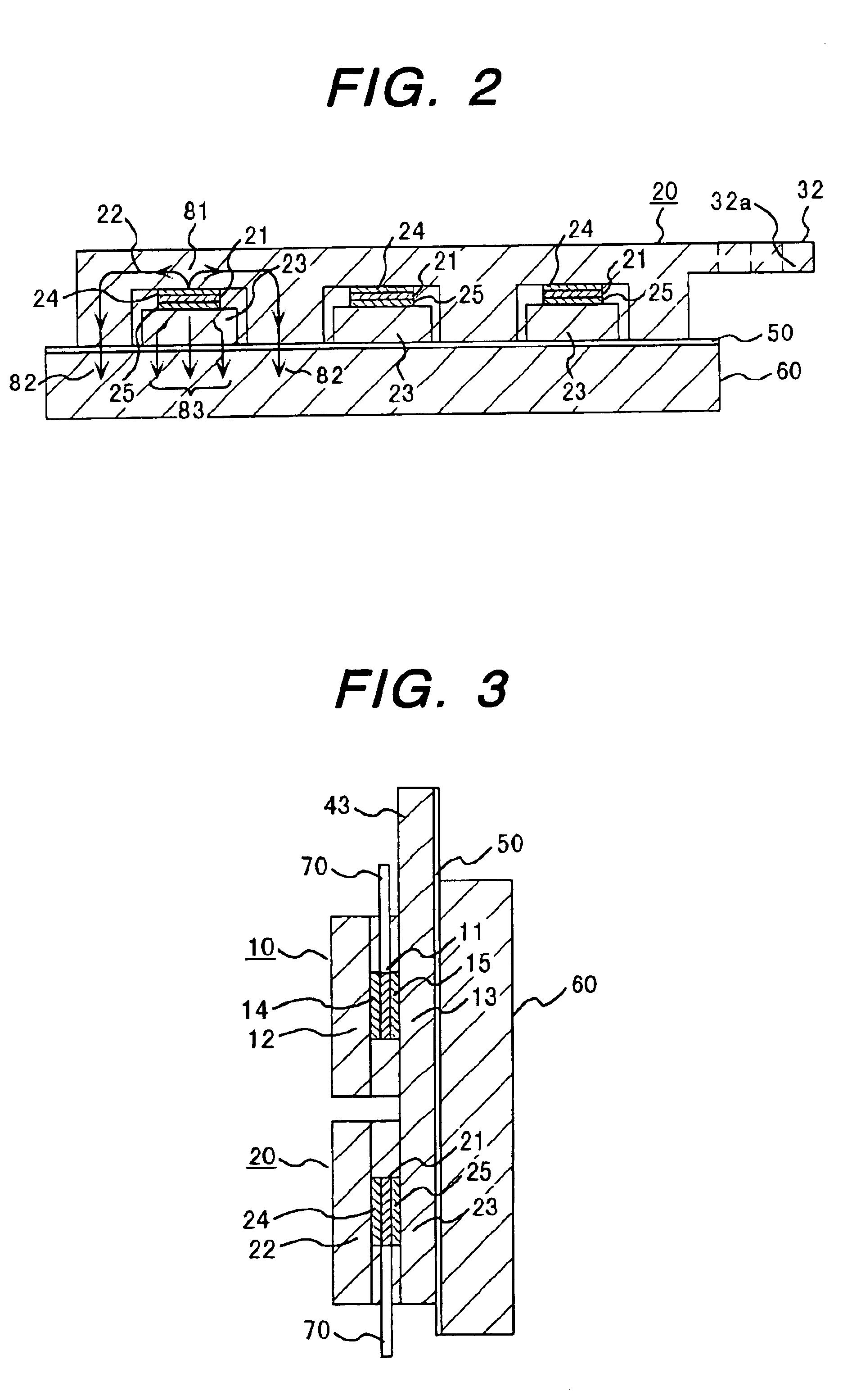
the present invention is described below in accordance with FIGS. 1 to 8. FIG. 8 shows the circuit composition of a power conversion device in the present embodiment. The power conversion device in the present embodiment is intended to be mounted in the motor-driving system of an automobile (for example, a motor-driving system for an electric automobile or a hybrid automobile, or a motor-driving system for automotive motor loads such as an air conditioner and brakes), and this power conversion device is described below taking as an example an inverter device 100 by which the DC power from a battery 200 (operating at, for example, a charging voltage of 42 V) is to be converted into three-phase AC power and then supplied to an AC motor 300 (for example, a synchronous motor, an induction motor, or the like).

The inverter device 100 is constructed so that the DC power of the battery 200 that has been supplied via a positive-pole DC bus 110 and a negative-pole DC bus 120 is first converte...


PUM


Abstract

One method of achieving the above subjects is by connecting one of electroconductive members 12, which are pre-connected to the top and bottom of a semiconductor chip 11 and have thermal conductivity, to an electroconductive member 13, which is used with the semiconductor chip 11 to constitute a laminated structure, in electrically insulated form on the same surface as the installation surface of the electroconductive member 13 so as to straddle the laminated structure constituted by the semiconductor chip 11 and the electroconductive member 13.

Description

BACKGROUND OF THE INVENTIONThe present invention relates to a semiconductor module and a power conversion device using the same.Some types of power conversion devices comprise a semiconductor module in which chip-like semiconductor devices are mounted in packaged IC form. A large majority of power conversion devices, however, comprise a semiconductor module in which semiconductor devices are mounted as they are. The latter is intended to improve the cooling effect of the semiconductor module by directly releasing the heat emitted from the semiconductor devices.Examples of the products known as semiconductor modules of this conventional type are disclosed in Japanese Laid-Open Patent Publication No. Hei 10-56131. Various products designed so that the heat emitted from the respective semiconductor chips is released from the two principal faces of each semiconductor chip are proposed in Japanese Laid-Open Patent Publication No. Hei 10-56131.These products include, for example, a semico...

Claims


Application Information

Patent Timeline
IPC IPC(8): H01L23/02H01L23/36H01L23/051H01L23/34H01L25/07H01L25/18H02M1/00H02M7/48
CPCH01L23/051H01L23/36H01L24/48H01L25/072H01L2924/1305H01L2224/48091H01L2924/01023H01L2924/00014H01L2924/3011H01L2924/13091H01L2924/13055H01L2924/10253H01L2924/014H01L2924/01082H01L2924/01074H01L2924/01047H01L2924/01033H01L2924/01029H01L2924/01014H01L2224/05599H01L2224/48095H01L2224/48247H01L2224/484H01L2224/85399H01L2924/01004H01L2924/01006H01L2924/01013H01L2224/45099H01L2924/00H01L2924/351
Inventor YOSHIZAKI, ATSUHIROMASHINO, KEIICHIANAN, HIROMICHIOCHIAI, YOSHITAKA
Owner HITACHI ASTEMO LTD
Learn More