Processing Liquid and Processing Method for Semiconductor Device, and Semiconductor Manufacturing Apparatus

Inactive Publication Date: 2007-10-04
TOHOKU UNIV +1
View PDF16 Cites 0 Cited by
  • Summary
  • Abstract
  • Description
  • Claims
  • Application Information

AI Technical Summary

Benefits of technology

[0034] According to this invention, by processing a surface of a semiconductor using an aqueous solution containing at least one kind of alcohols and ketones, it is possible to suppress dissolution of semiconductor constituent atoms from the semiconductor surface to 15 atomic layers / 24 hours or less. Further, the surface roughness of the semiconductor after the processing can be set to 0.10 nm or less as compared with a surface roughness of about 1.0 nm obtained by the conventional RCA cleaning technique. Therefore, the improvement in performance of a semiconductor device can be expected. Further, by filling a processing atmosphere with a proper gas, there is an effect of suppressing formation of a film such as a natural oxide film that causes deterioration in properties of a semiconductor device.
[0035] Further, according to this invention, by providing a step of removing alcohols and ketones adhering to a semiconductor surface after processing the semiconductor surface using an aqueous solution containing at least one kind of alcohols and ketones, there occurs no deterioration in properties such as lowering of a dielectric-breakdown electric field caused by adhered alcohols remaining in a structure stacked on the semiconductor surface, which has been a problem in the conventional semiconductor manufacturing technique using alcohol. Further, by the use of a plasma excited by a microwave, there is obtained a similar processing effect at a lower temperature as compared with a conventional removal method using heat.
[0036] Furthermore, according to this invention, by recovering a processing liquid used in processing a semiconductor surface with an aqueous solution containing at least one kind of alcohols and reusing it after purification, the amount of use of alcohol can be reduced.
[0037] According to a processing liquid and a processing method for a semiconductor device, and a semiconductor manufacturing apparatus of the invention of this application, there are obtained the processing liquid, the processing method, and the semiconductor manufacturing apparatus that realize a process with only a little dissolution from a semiconductor surface and a clean and flat surface.

Problems solved by technology

It has been pointed out that the surface roughness of semiconductor surfaces or semiconductor oxide film / semiconductor interfaces causes deterioration in properties of electronic elements such as MOS devices.
While the influence of the surface roughness to the device properties has not been actualized in the manufacture of devices having relatively large sizes, it is becoming unignorable due to a reduction in thickness of MOSFET gate oxide films and so on following the miniaturization of devices in recent years.
However, since the surface roughness of a semiconductor increases according to this cleaning method, a problem has arisen in the manufacture of current semiconductor integrated circuit devices in which it is necessary to form a silicon oxide film having a thickness of 100 Å or less.
Rather, the surface roughness is deteriorated due to a chemical reaction between the semiconductor surface and the water in the water.
However, it is obvious that the miniaturization of semiconductor devises will further advance in future and it is sure to be a problem then.
Therefore, the technique is limited in use and thus is not applicable to the comprehensive semiconductor manufacture.
Particularly, it is not a technique that enables the surface of a semiconductor before formation of a semiconductor oxide film to be extremely clean and flat.

Method used


Image

  • Processing Liquid and Processing Method for Semiconductor Device, and Semiconductor Manufacturing Apparatus
  • Processing Liquid and Processing Method for Semiconductor Device, and Semiconductor Manufacturing Apparatus
  • Processing Liquid and Processing Method for Semiconductor Device, and Semiconductor Manufacturing Apparatus

Examples


embodiment 1

[0056] The embodiment 1 of this invention is such that an aqueous solution adapted to cause a dissolution amount of atoms from a semiconductor substrate to be 15 atomic layers / 24 hours or less by conversion is used when processing the semiconductor substrate, thereby improving a processing liquid and a processing method. In the embodiment 1, description will be made of these processing liquid and processing method and a semiconductor manufacturing apparatus using them in the manufacture of a semiconductor device.

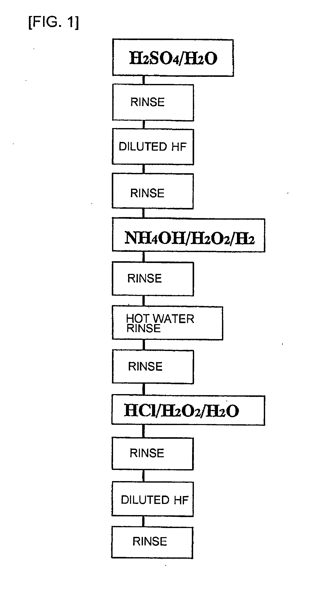
[0057] This invention is applicable to various process sequences that are based on features of various processing liquids currently used in the semiconductor manufacturing processes. FIG. 1 shows one example of an RCA cleaning method as a processing process. The various process sequences each use a treatment with a water rinse as a rinsing process and this invention proposes a method of improving those water rinsing processes. Therefore, this invention is not limited to a p...

embodiment 2

[0062] The embodiment 2 of this invention is characterized by comprising a step of removing alcohols and ketones adhering to a semiconductor surface after processing a semiconductor substrate using an aqueous solution containing at least one or more kinds of alcohols and ketones. In the embodiment 2, description will be made of a processing method and a semiconductor manufacturing apparatus in the case where there are applied a treatment using a processing liquid containing at least one or more kinds of alcohols and ketones and an alcohol / ketone removal step thereafter in the manufacture of a semiconductor device.

[0063] As alcohols and ketones to be used, there can be cited, as examples, methanol, ethanol, 1-propanol, 2-propanol, 1-butanol, 2-butanol, tert-butyl alcohol, 1-pentanol, 2-pentanol, acetone, diethyl ketone, ethyl methyl ketone, and so on. If the following conditions are satisfied, for example, 1,3-fluoro-2-propanol and difluoromethyl ketone may be cited as alcohol and k...

embodiment 3

[0074] The embodiment 3 is a processing method characterized by recovering a processing liquid used in a processing step and reusing it after purification. Description will be made of a configuration in which a mechanism therefor is added to the semiconductor manufacturing process.

[0075]FIG. 6 is a schematic diagram of the processing process having the foregoing processing liquid recovery purification mechanism. Part of the semiconductor manufacturing process is extracted and shown at 1 to 4 in FIG. 6. In this invention, a processing liquid used at 3 in FIG. 6 is recovered to a purification step at 6 in FIG. 6. After the recovery, the recovered processing liquid is adjusted to a composition, in a rinsing liquid adjusting step at 5 in FIG. 6, suitable for a subsequent step and then it is reused.

[0076] The purpose of the purification is to remove the impurities. Ultrafiltration, reverse osmosis membrane, or the like can be used for particulate impurities. Metal impurities can be rem...


PUM


Abstract

Disclosed is a process liquid which causes only little dissolution of atoms from a semiconductor surface and enables to form a clean and flat semiconductor surface. Also disclosed are a processing method and an apparatus for manufacturing a semiconductor. Specifically disclosed is a process liquid-which causes only little dissolution of atoms from a semiconductor surface by using an aqueous solution containing at least one alcohol or ketone, thereby realizing a clean and flat surface.

Description

TECHNICAL FIELD [0001] This invention relates to a processing liquid and a processing method for a semiconductor device, and a semiconductor manufacturing apparatus and, in particular, relates to a processing liquid and a processing method for a semiconductor device, that can form a clean and flat semiconductor surface, and a semiconductor manufacturing apparatus that can form a clean and flat semiconductor surface. BACKGROUND ART [0002] It has been pointed out that the surface roughness of semiconductor surfaces or semiconductor oxide film / semiconductor interfaces causes deterioration in properties of electronic elements such as MOS devices. While the influence of the surface roughness to the device properties has not been actualized in the manufacture of devices having relatively large sizes, it is becoming unignorable due to a reduction in thickness of MOSFET gate oxide films and so on following the miniaturization of devices in recent years. [0003] The RCA cleaning including nea...

Claims


Application Information

Patent Timeline
IPC IPC(8): B08B3/00C11D9/44H01L21/302
CPCH01L21/02063H01L21/304H01L21/308
Inventor OHMITERAMOTO, AKINOBUKIKUYAMA, HIROHISANII, KEIICHIYAMAMOTO, MASASHI
Owner TOHOKU UNIV
Why Eureka
Try Eureka