Method for sealing an active area of a surface acoustic wave device on a wafer

a surface acoustic wave and active area technology, applied in the field of integrated circuit fabrication process and structure, can solve the problems of temperature dependent change in acoustic wave velocity, degrade device performance, and alter device performan

Inactive Publication Date: 2005-04-12
SILICON LIGHT MACHINES CORP
View PDF41 Cites 22 Cited by
  • Summary
  • Abstract
  • Description
  • Claims
  • Application Information

AI Technical Summary

Benefits of technology

These and other features of the present invention will be readily apparent to persons of ordinary skill in the art upon reading the entirety of this disclosure, which includes the accompanying drawings and claims.

Problems solved by technology

One problem encountered with SAW devices is that the regions of the device where the acoustic waves are present can be very sensitive to the presence of surface contaminants that alter the wave velocities and consequently degrade the device performance.
Even a monolayer of contaminant on the surface of the crystal can noticeably alter the device performance.
Another problem associated with SAW devices is that a change in acoustic wave velocity is temperature dependent.
This temperature dependence effectively limits the operable temperature range of SAW devices.

Method used


Image

  • Method for sealing an active area of a surface acoustic wave device on a wafer
  • Method for sealing an active area of a surface acoustic wave device on a wafer
  • Method for sealing an active area of a surface acoustic wave device on a wafer

Examples


Embodiment Construction

The above described problems and difficulties with SAW devices (and similar problems with other non-silicon-based devices) may be overcome by controlling the atmosphere in which the devices operate.

One way to achieve this would be to seal the devices on the packaging level during packaging of the individual die. Seals may be formed, for example, in metal or ceramic packages. For instance, a metal package may be welded or soldered to seal it, and the individual leads may be sealed using separate glass seals to separate the leads from the metal. As another example, in ceramic packages, a metal seal band attached by glassy material may be used to facilitate the sealing by welding or soldering, and the leads may be embedded in the ceramic itself. Other types of packages and other sealing techniques at the packaging level may also be used.

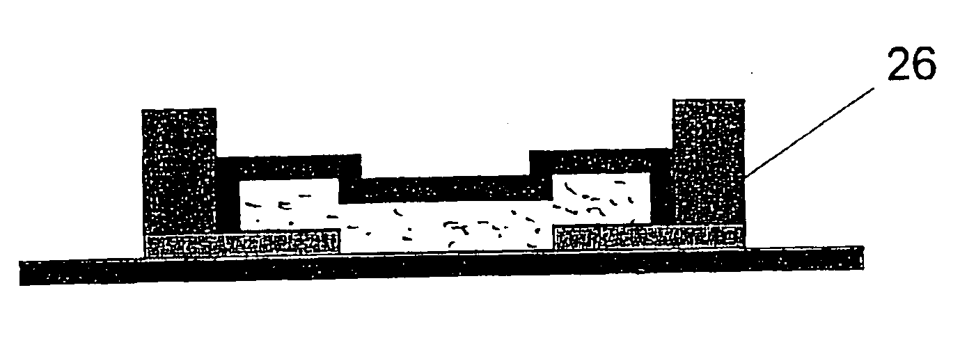
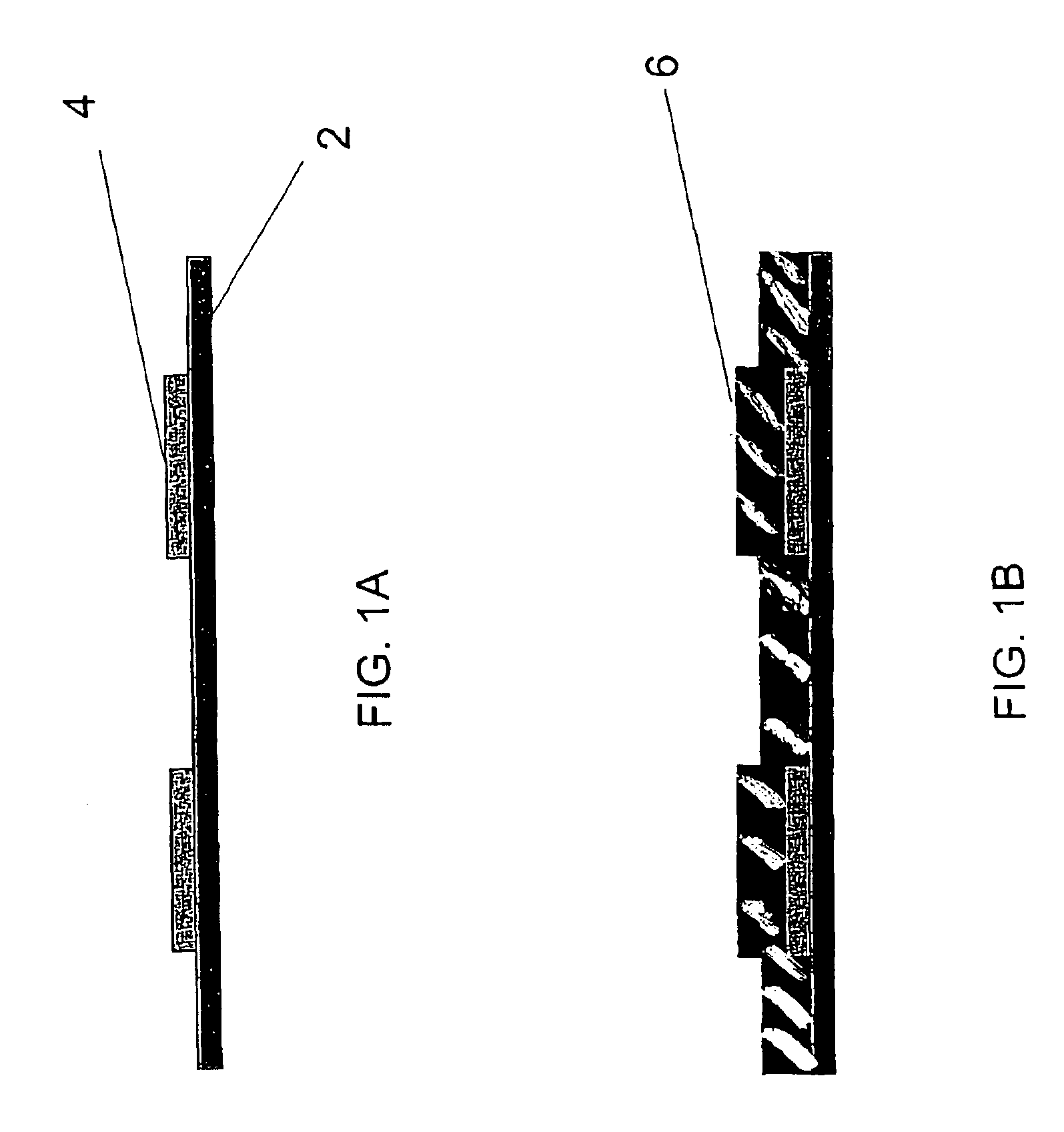
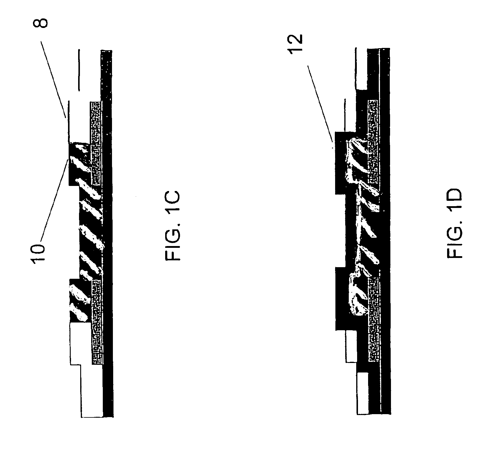
As disclosed in detail in the present application, a different and advantageous way to control the atmosphere in which the SAW device operates is to fa...


PUM

PropertyMeasurementUnit
feature sizeaaaaaaaaaa
sizesaaaaaaaaaa
sizesaaaaaaaaaa

Abstract

One embodiment disclosed relates to a method for sealing an active area of a surface acoustic wave (SAW) device on a wafer. The method includes providing a sacrificial material over at least the active area of the SAW device, depositing a seal coating over the wafer so that the seal coating covers the sacrificial material, and replacing the sacrificial material with a target atmosphere. Another embodiment disclosed relates to an SAW device sealed at the wafer level (i.e. prior to separation of the die from the wafer). The device includes an active area to be protected, an electrical contact area, and a lithographically-formed structure sealing at least the active area and leaving at least a portion of the electrical contact area exposed.

Description

REFERENCE TO RELATED APPLICATIONThe present application is related to “Wafer-Level Seal for Non-Silicon-Based Devices,” filed on the same date herewith, by inventors Gregory D. Miller and Mike Bruner (Silicon Light Machines docket # P0277).BACKGROUND OF THE INVENTION1. Field of the InventionThe present invention relates generally to integrated circuits, and more particularly to integrated circuit fabrication processes and structures.2. Description of the Background ArtSurface acoustic wave (SAW) devices are often used in communication devices, such as, for example, radio frequency (RF) filters in mobile phone handsets and communication networks. SAW devices utilize waves that propagate along the surface (or near surface) of a substrate. As used herein, SAW devices include those that utilize piezoelectrically-coupled Rayleigh waves and may also include those that utilize non-Rayleigh (skimming or “leaky”) waves.A typical SAW filter includes input and output transducers formed on a no...

Claims


Application Information

Patent Timeline
Patent Type & Authority Patents(United States)
IPC IPC(8): B81B7/00H03H3/08H03H9/02H03H3/00
CPCB81C1/00293H03H3/08H03H9/02921H03H9/02984H03H9/1092B81C2203/0136Y10T29/49011Y10T428/12521Y10T29/4908Y10T29/49005Y10T29/4902Y10T29/49007Y10T29/42
Inventor MILLER, GREGORY D.BRUNER, MIKERAGAN, LAWRENCE HENRYGREEN, GARY
Owner SILICON LIGHT MACHINES CORP
Why Eureka
Try Eureka