Photoelectric conversion device, and image sensor and image input system making use of the same

a conversion device and photoelectric technology, applied in the direction of diodes, semiconductor devices, radio frequency controlled devices, etc., can solve the problems of reducing the capacitance at the photoelectric conversion area, reducing the image quality, and increasing the reset noise produced when a photodetector is reset, so as to achieve the effect of large capacitan

Inactive Publication Date: 2005-04-12
CANON KK
View PDF22 Cites 25 Cited by
  • Summary
  • Abstract
  • Description
  • Claims
  • Application Information

AI Technical Summary

Benefits of technology

In the photoelectric conversion device, the conductor, which serve as a shield, may comprise a conductor extending into a substantially square opening formed in a light-screen

Problems solved by technology

In general, the reset noise produced when a photodetector is reset increases with a decrease in capacitance at the photoelectric conversion area.
However, in such a photoelectric conversion device in which the noise signals occurring immediately after the resetting of a photodetector are retained during accumulation and subtracted from light signals to eliminate the reset noise of the photodetector, some external noises radiated from the outside of the photoelectric conversion device, in particular, low-frequency noises such as power-source noise may lower image quality.
However, once, e.g., a low-frequency noise of about 50 Hz radiated from a power source of an ins

Method used


Image

  • Photoelectric conversion device, and image sensor and image input system making use of the same
  • Photoelectric conversion device, and image sensor and image input system making use of the same
  • Photoelectric conversion device, and image sensor and image input system making use of the same

Examples


embodiment 1

(Embodiment 1)

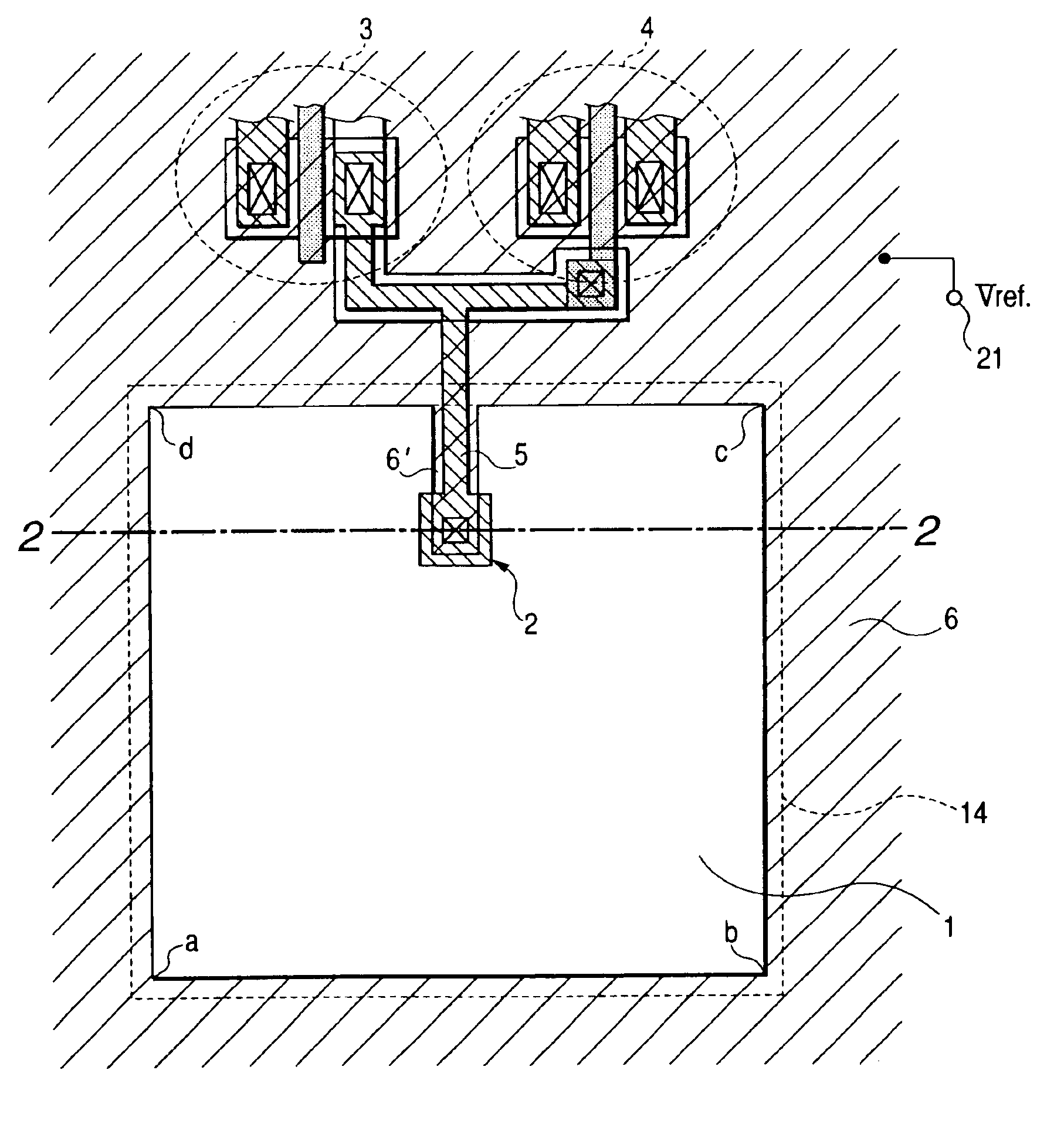
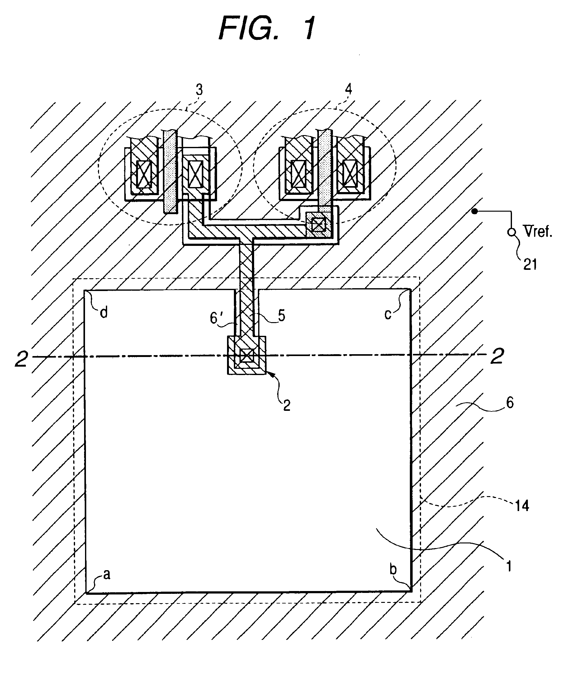
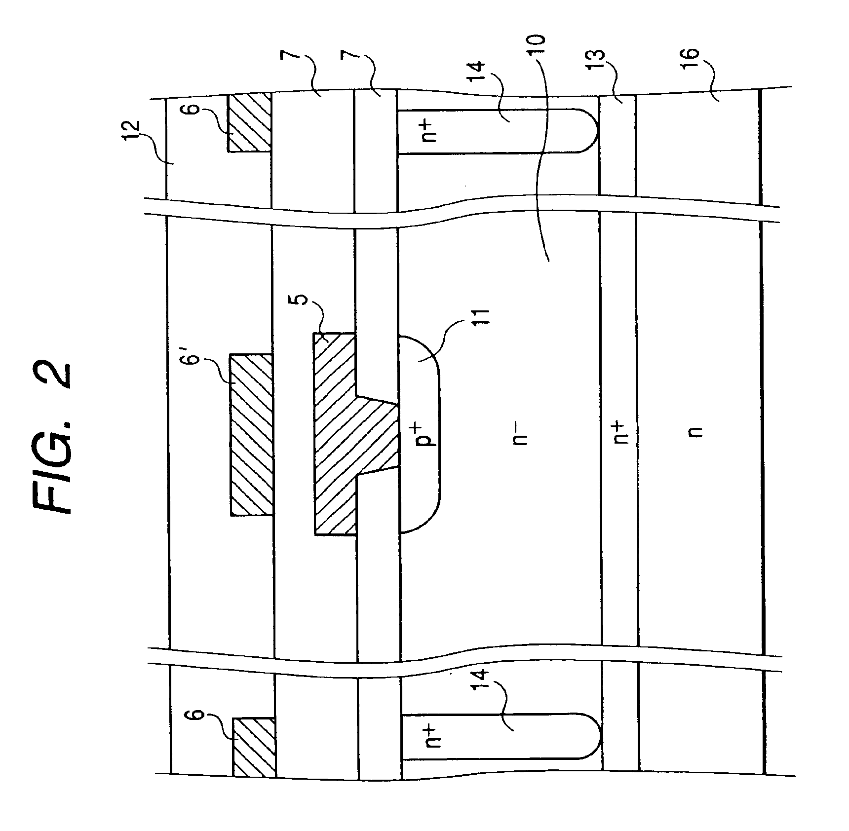
FIG. 1 illustrates a planar structure of a photodetector as a photoelectric conversion device according to the present invention. FIG. 2 illustrates a cross-sectional structure along the line 2-2 in FIG.

The photoelectric conversion device according to the present embodiment comprises:

an n−-type region 10 as a first-conductivity type first semiconductor region, located in a pixel region (a pixel region opening; hereinafter merely “opening”) 1;

a p+-type region 11 as a second-conductivity type second semiconductor region, provided in the first semiconductor region 10, where in a floating state, the first semiconductor region 10 may accumulate photoelectric carriers therein;

a wiring 5 for electrically connecting the second semiconductor region 11 to circuit elements 3 and 4 located outside the pixel region 1; and

a conductor 6′ provided on the wiring 5 located inside the pixel region, via an insulator 7 and kept at a stated potential.

The conductor 6′ stands extended into th...


PUM


Abstract

In a photoelectric conversion device comprising a first-conductivity type first semiconductor region located in a pixel region, a second-conductivity type second semiconductor region provided in the first semiconductor region, and a wiring for electrically connecting the second semiconductor region to a circuit element located outside the pixel region, a shield is provided on the light-incident side of the wiring, via an insulator in such a way that it covers at least part of the wiring and also the shield comprises a conductor whose potential stands fixed.
This photoelectric conversion device may hardly be affected with low-frequency radiated noises as typified by power-source noise.

Description

BACKGROUND OF THE INVENTION1. Field of the InventionThis invention relates to an image scanner, a facsimile transmission system and other image input systems, or image sensors of various types, and a photoelectric conversion device (or photoelectric transducer) used in them. More particularly, it relates to an improvement of pixel (picture element) structure.2. Related Background ArtPhotoelectric conversion devices are widely used in the above image input systems and image sensors.As generally known examples, CCD image sensors making use of a reduction optical system and non-reduction contact type image sensors multiple-mounted with a plurality of semiconductor photosensor chips are used in, e.g., image scanners for inputting images. These are being developed energetically.As photodetectors used as photoelectric conversion devices in these systems and sensors, it is common to use photodiodes comprising a semiconductor p-n junction. For example, as disclosed in Japanese Patent Applic...

Claims


Application Information

Patent Timeline
IPC IPC(8): H01L27/146H01L31/0264H01L31/0328H01L31/062
CPCH01L27/14623H01L27/14643H01L27/14609H01L2224/48091H01L2924/3025H01L2924/13091H01L2924/3011H01L2924/00014H01L2924/00
Inventor KOZUKA, HIRAKUKAIHOTSU, TAKAHIRO
Owner CANON KK
Why Eureka
Try Eureka